
Datasheet


SN65MLVD047A
SLLS736A − JULY 2006 − REVISED MAY 2008
www.ti.com
4
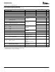
ELECTRICAL CHARACTERISTICS
over recommended operating conditions unless otherwise noted
PARAMETER TEST CONDITIONS MIN
(1)
TYP
(2)
MAX UNIT
LVTTL (EN, EN, 1A:4A)
|I
IH
|
High-level input current V
IH
= 2 V or V
CC
0 10 µA
|I
IL
|
Low-level input current V
IL
= GND or 0.8 V
0 10 µA
C
i
Input capacitance V
I
= 0.4 sin(30E6πt) + 0.5 V
(3)
5 pF
M−LVDS (1Y/1Z:4Y/4Z)
⎪V
YZ
⎪
Differential output voltage magnitude
480 650 mV
∆⎪V
YZ
⎪
Change in differential output voltage magnitude
between logic states
See Figure 2
−50 50 mV
V
OS(SS)
Steady-state common-mode output voltage
0.8 1.2 V
∆V
OS(SS)
Change in steady-state common-mode output
voltage between logic states
See Figure 3
−50 50 mV
V
OS(PP)
Peak-to-peak common-mode output voltage
150 mV
V
Y(OC)
Maximum steady-state open-circuit output
voltage
See Figure 7
0 2.4 V
V
Z(OC)
Maximum steady-state open-circuit output
voltage
See Figure 7
0 2.4 V
V
P(H)
Voltage overshoot, low-to-high level output
See Figure 5
1.2 V
SS
V
V
P(L)
Voltage overshoot, high-to-low level output
See Figure 5
−0.2 V
SS
V
⎪I
OS
⎪
Differential short-circuit output current magnitude See Figure 4
24 mA
I
OZ
High-impedance state output current
−1.4 V ≤ (V
Y
or V
Z
)≤ 3.8 V,
Other output = 1.2 V
−15 10 µA
I
O(OFF)
Power-off output current
−1.4 V ≤ (V
Y
or V
Z
)≤ 3.8 V,
Other output = 1.2 V,
V
CC
= 1.5 V
−10 10 µA
C
Y
or C
Z
Output capacitance
V
Y
or V
Z
= 0.4 sin(30E6πt) +
0.5 V,
(3)
Other outputs at 1.2 V, driver
disabled
3 pF
C
YZ
Differential output capacitance
V
YZ
= 0.4 sin(30E6πt) V,
(3)
Driver disabled
2.5 pF
C
Y/Z
Output capacitance balance, (C
Y
/C
Z
)
0.99 1.01
(1)
The algebraic convention, in which the least positive (most negative) limit is designated as minimum is used in this data sheet.
(2)
All typical values are at 25°C and with a 3.3-V supply voltage.
(3)
HP4194A impedance analyzer (or equivalent)