
Datasheet


www.ti.com
SN65LVDSxxxx ELECTRICAL CHARACTERISTICS
SN65LVDSxxxx SWITCHING CHARACTERISTICS
SN55LVDS31, SN65LVDS31
SN65LVDS3487, SN65LVDS9638
SLLS261L – JULY 1997 – REVISED JULY 2007
over recommended operating conditions (unless otherwise noted)
SN65LVDS31
SN65LVDS3487
PARAMETER TEST CONDITIONS UNIT
SN65LVDS9638
MIN TYP
(1)
MAX
V
OD
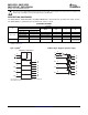
Differential output voltage magnitude R
L
= 100 Ω , See Figure 2 247 340 454 mV
Change in differential output voltage
Δ V
OD
R
L
= 100 Ω , See Figure 2 –50 50 mV
magnitude between logic states
1.37
V
OC(SS)
Steady-state common-mode output voltage See Figure 3 1.125 1.2 V
5
Δ V
OC(S
Change in steady-state common-mode output
See Figure 3 –50 50 mV
S)
voltage between logic states
V
OC(PP)
Peak-to-peak common-mode output voltage See Figure 3 50 150 mV
V
I
= 0.8 V or 2 V, Enabled, No load 9 20
SN65LVDS31,
V
I
= 0.8 or 2 V, R
L
= 100 Ω , Enabled 25 35 mA
SN65LVDS3487
I
CC
Supply current V
I
= 0 or V
CC
, Disabled 0.25 1
No load 4.7 8
SN65LVDS9638 V
I
= 0.8 V or 2 V mA
R
L
= 100 Ω 9 13
I
IH
High-level input current V
IH
= 2 4 20 μ A
I
IL
Low-level input current V
IL
= 0.8 V 0.1 10 μ A
V
O(Y)
or V
O(Z)
= 0 –4 –24
I
OS
Short-circuit output current mA
V
OD
= 0 ± 12
I
OZ
High-impedance output current V
O
= 0 or 2.4 V ± 1 μ A
I
O(OFF)
Power-off output current V
CC
= 0, V
O
= 2.4 V ± 1 μ A
C
i
Input capacitance 3 pF
(1) All typical values are at T
A
= 25 ° C and with V
CC
= 3.3 V.
over recommended operating conditions (unless otherwise noted)
SN65LVDS31
SN65LVDS3487
PARAMETER TEST CONDITIONS UNIT
SN65LVDS9638
MIN TYP
(1)
MAX
t
PLH
Propagation delay time, low-to-high-level output 0.5 1.4 2 ns
t
PHL
Propagation delay time, high-to-low-level output 1 1.7 2.5 ns
t
r
Differential output signal rise time (20% to 80%) 0.4 0.5 0.6 ns
R
L
= 100 Ω , C
L
= 10 pF,
See Figure 2
t
f
Differential output signal fall time (80% to 20%) 0.4 0.5 0.6 ns
t
sk(p)
Pulse skew (|t
PHL
– t
PLH
|) 0.3 0.6 ns
t
sk(o)
Channel-to-channel output skew
(2)
0 0.3 ns
t
sk(pp)
Part-to-part skew
(3)
800 ps
t
PZH
Propagation delay time, high-impedance-to-high-level output 5.4 15 ns
t
PZL
Propagation delay time, high-impedance-to-low-level output 2.5 15 ns
See Figure 4
t
PHZ
Propagation delay time, high-level-to-high-impedance output 8.1 15 ns
t
PLZ
Propagation delay time, low-level-to-high-impedance output 7.3 15 ns
(1) All typical values are at T
A
= 25 ° C and with V
CC
= 3.3 V.
(2) t
sk(o)
is the skew between specified outputs of a single device with all driving inputs connected together and the outputs switching in the
same direction while driving identical specified loads.
(3) t
sk(pp)
is the magnitude of the difference in propagation delay times between any specified terminals of two devices when both devices
operate with the same supply voltages, same temperature, and have identical packages and test circuits.
7
Submit Documentation Feedback