
Datasheet


www.ti.com
10
1
0.1
Transmission Distance − m
100
Signaling Rate − Mbps
10 100 1000
5% Jitter
(see Note A)
30% Jitter
(see Note A)
24 AWG UTP 96 Ω
(PVC Dielectric)
TRANSMISSION DISTANCE
vs
SIGNALING RATE
1B
1A
1Y
G
2Y
2A
2B
GND
V
CC
4B
4A
4Y
G
3Y
3A
3B
1
2
3
4
5
6
7
8
16
15
14
13
12
11
10
9
100 Ω
100 Ω
100 Ω
(see Note B)
100 Ω
3.3 V
0.1 µF
(see Note A)
0.001 µF
(see Note A)
V
CC
See Note C
SN55LVDS32 , SN65LVDS32
SN65LVDS3486 , SN65LVDS9637
SLLS262Q – JULY 1997 – REVISED JULY 2007
APPLICATION INFORMATION (continued)
A. This parameter is the percentage of distortion of the unit interval (UI) with a pseudorandom data pattern.
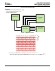
Figure 15. Typical Transmission Distance Versus Signaling Rate
A. Place a 0.1- μ F and a 0.001- μ F Z5U ceramic, mica, or polystyrene dielectric, 0805 size, chip capacitor between V
CC
and the ground plane. The capacitors should be located as close as possible to the device terminals.
B. The termination resistance value should match the nominal characteristic impedance of the transmission media with
± 10%.
C. Unused enable inputs should be tied to V
CC
or GND as appropriate.
Figure 16. Typical Application Circuit Schematic
16
Submit Documentation Feedback