
Datasheet


www.ti.com
DESCRIPTION (CONTINUED)
’LVDS31 logic diagram (positive logic)
4Z
4Y
3Z
3Y
2Z
2Y
1Z
1Y
13
14
11
10
5
6
3
2
4A
3A
2A
1A
G
G
15
9
7
1
12
4
logic symbol
†
SN55LVDS31, SN65LVDS31
4Z
4Y
3Z
3Y
2Z
2Y
1Z
1Y
4A
3A
2A
1A
G
G
13
14
11
10
5
6
3
2
15
9
7
1
12
4
≥ 1
EN
†
This symbol is in accordance with ANSI/IEEE Std 91-1984 and
IEC Publication 617-12.
SN55LVDS31, SN65LVDS31
SN65LVDS3487, SN65LVDS9638
SLLS261L – JULY 1997 – REVISED JULY 2007
These devices have limited built-in ESD protection. The leads should be shorted together or the device placed in conductive foam
during storage or handling to prevent electrostatic damage to the MOS gates.
The SN65LVDS31, SN65LVDS3487, and SN65LVDS9638 are characterized for operation from –40 ° C to 85 ° C.
The SN55LVDS31 is characterized for operation from –55 ° C to 125 ° C.
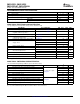
AVAILABLE OPTIONS
PACKAGE
(1)
T
A
SMALL OUTLINE
CHIP CARRIER CERAMIC DIP FLAT PACK
MSOP
(FK) (J) (W)
(D) (PW)
SN65LVDS31D SN65LVDS31PW — — — —
SN65LVDS3487D — — — — —
–40 ° C to 85 ° C
SN65LVDS9638D — SN65LVDS9638DGN — — —
— — SN65LVDS9638DGK — — —
SNJ55LVDS31W
–55 ° C to 125 ° C — — — SNJ55LVDS31FK SNJ55LVDS31J
SN55LVDS31W
(1) For the most current package and ordering information, see the Package Option Addendum at the end of this document, or see the TI
website at www.ti.com .
2
Submit Documentation Feedback