
Datasheet


Image
Sensor
FPC
SN65LVDS315
OMAP2420
0.1 Fm
0.1 Fm
1.8V 1.8Vto3.3V
1.8V
GND
1.8V
GND
88MHz
88Mbps
ccp_clkp
ccp_clkn
ccp_datap
ccp_datan
cam_xclk
I2C
2
1.8Vto3.3V
2
8
MODE
TXEN
GND
HS,VS
D[0:7]
DCLK
VDDPLLD
VDDLVDS
VDDPLLA
VDD
CLK+
CLK-
DOUT+
DOUT-
11MHz
PixelCLK
HS,VS
D[0:7]
REFCLK
I2C
SerialInterface
SN65LVDS315
www.ti.com
SLLS881F –DECEMBER 2007–REVISED SEPTEMBER 2012
POWER SUPPLY DESIGN RECOMMENDATION
For a multilayer PCB, it is recommended to keep one common GND layer underneath the device and connect all
ground terminals directly to this plane.
SN65LVDS315 DECOUPLING RECOMMENDATION
The SN65LVDS315 was designed to operate reliably in a constricted environment with other digital switching
ICs. In cell phone designs, the SN65LVDS315 often shares a power supply with various other ICs. The
SN65LVDS315 can operate with power supply noise as specified in Recommend Device Operating Conditions.
To minimize the power supply noise floor, provide good decoupling near the SN65LVDS315 power pins. The use
of four ceramic capacitors (two 0.01 μF and two 0.1 μF) provides good performance. At the very least, it is
recommended to install one 0.1 μF and one 0.01 μF capacitor near the SN65LVDS315. To avoid large current
loops and trace inductance, the trace length between decoupling capacitor and IC power inputs pins must be
minimized. Placing the capacitor underneath the SN65LVDS315 on the bottom of the pcb is often a good choice.
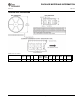
VGA CAMERA APPLICATION
Figure 27 shows a possible implementation of a 10-Mpixel camera transfer with 30Hz frame refresh rate. The
SN65LVDS315 interfaces to the OMAP2420, a TI application processor with integrated CSI receiver. The pixel
clock rate is 11 MHz, assuming ≈20% blanking overhead. The application assumes 8-bit color resolution.
Figure 27. Typical VGA Display Application
TYPICAL APPLICATION FREQUENCIES
The SN65LVDS315 in display mode supports pixel clock frequencies from 7 MHz to 27 MHz (which translates to
DCLK frequencies of 56 MHz to 208 MHz). Table 9 provides a few typical display resolution examples. The table
also shows the assumed blanking overhead, which often times is smaller in the final application, resulting in a
lower data rate.
Copyright © 2007–2012, Texas Instruments Incorporated Submit Documentation Feedback 25
Product Folder Links :SN65LVDS315