
Datasheet


www.ti.com
SN65LVDS049
SLLS575–AUGUST 2003
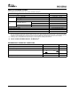
SWITCHING CHARACTERISTICS
over operating free-air temperature range (unless otherwise noted)
PARAMETER TEST CONDITIONS MIN TYP
(1)
MAX UNIT
LVDS Outputs (D
OUT+
, D
OUT-
)
t
PLHD
Differential propagation delay low to high R
L
= 100 Ω, 1.3 2.0 ns
C
L
= 15 pF distributed,
t
PHLD
Differential propagation delay high to low 1.4 2.0 ns
See Figure 2
t
sk(p)
Differential pulse skew (|t
PHL
- t
PLH
|) 0 0.15 0.4 ns
t
sk(o)
Differential channel-to-channel skew
(2)
0 0.05 0.5 ns
t
sk(pp)
Differential part-to-part skew
(3)
0 1 ns
t
r
Differential rise time 0.2 0.5 1 ns
t
f
Differential fall time 0.2 0.5 1 ns
t
PHZ
Disable time, high level to high impedance R
L
= 100 Ω, 2.7 4 ns
C
L
= 15 pF distributed,
t
PLZ
Disable time, low level to high impedance 2.7 4 ns
See Figure 3
t
PZH
Enable time, high impedance to high level 1 5 8 ns
t
PZL
Enable time, high impedance to low level 1 5 8 ns
f
MAX
Maximum operating frequency
(4)
250 MHz
LVCMOS Outputs (R
OUT
)
t
PLH
Propagation delay low to high V
ID
= 200 mV, 0.5 1.9 3.5 ns
C
L
= 15 pF distributed,
t
PHL
Propagation delay high to low 0.5 1.7 3.5 ns
See Figure 4
t
sk(p)
Pulse skew (|t
PHL
- t
PLH
|) 0 0.2 0.4 ns
t
sk(o)
Channel-to-channel skew
(5)
0 0.05 0.5 ns
t
sk(pp)
Part-to-part skew
(6)
0 1 ns
t
r
Rise time 0.3 0.5 1.4 ns
t
f
Fall time 0.3 0.5 1.4 ns
t
PHZ
Disable time, high level to high impedance C
L
= 15 pF distributed, 3 7.2 9 ns
See Figure 5
t
PLZ
Disable time, low level to high impedance 2.5 4 8 ns
t
PZH
Enable time, high impedance to high level 2.5 4.2 7 ns
t
PZL
Enable time, high impedance to low level 2 3.3 7 ns
f
MAX
Maximum operating frequency
(7)
200 250 MHz
(1)
All typical values are at 25°C and with a 3.3 V supply.
(2)
t
sk(o)
is the magnitude of the time difference between the t
PLH
or t
PHL
of all drivers of a single device with all of their inputs connected
together.
(3)
t
sk(pp)
is the magnitude of the difference in propagation delay times between any specified terminals of two devices when both devices
operate with the same supply voltages, at the same temperature, and have identical packages and test circuits.
(4)
f
(MAX)
generator input conditions: t
r
= t
f
< 1 ns (0% to 100%), 50% duty cycle, 0 V to 3 V. Output Criteria: duty cycle = 45% to 55%, V
OD
> 250 mV, all channels switching.
(5)
t
sk(lim)
is the maximum delay time difference between drivers over temperature, V
CC
, and process.
(6)
tsk(pp) is the magnitude of the difference in propagation delay times between any specified terminals of two devices when both
devices operate wf(MAX) generaith the same supply voltages, at the same temperature, and have identical packages and test circuits
(7)
f
(MAX)
generator input conditions: t
r
= t
f
< 1 ns (0% to 100%), 50% duty cycle, V
ID
= 200 mV, V
CM
= 1.2 V. Output criteria: duty cycle =
45% to 55%, V
OH
> 2.7 V, V
OL
< 0.25 V, all channels switching.
5