
Datasheet


SN65HVDA1050A-Q1
SLLS994A –FEBRUARY 2010–REVISED DECEMBER 2010
www.ti.com
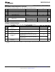
ABSOLUTE MAXIMUM RATINGS
(1)
1.1 V
CC
Supply voltage range
(2)
–0.3 V to 6 V
1.2 Voltage range at any bus terminal [CANH, CANL, SPLIT (V
REF
)] –27 V to 40 V
1.3 I
O
Receiver output current 20 mA
1.4 V
I
Voltage input range, ISO 7637 transient pulse
(3)
(CANH, CANL) –150 V to 100 V
1.5 V
I
Voltage input range (TXD, S) –0.3 V to 6 V
1.6 T
J
Junction temperature range –40°C to 150°C
(1) Stresses beyond those listed under "absolute maximum ratings" may cause permanent damage to the device. These are stress ratings
only and functional operation of the device at these or any other conditions beyond those indicated under "recommended operating
conditions" is not implied. Exposure to absolute-maximum-rated conditions for extended periods may affect device reliability.
(2) All voltage values, except differential I/O bus voltages, are with respect to network ground terminal.
(3) Tested in accordance with ISO 7637 test pulses 1, 2, 3a, 3b per IBEE system level test (Pulse 1 = –100 V, Pulse 2 = 100 V,
Pulse 3a = –150 V, Pulse 3b = 100 V). If dc may be coupled with ac transients, externally protect the bus pins within the absolute
maximum voltage range at any bus terminal. This device has been tested with dc bus shorts to +40V with leading common-mode
chokes. If common-mode chokes are used in the system and the bus lines may be shorted to dc, ensure that the choke type and value
in combination with the node termination and shorting voltage either will not create inductive flyback outside of voltage maximum
specification or use an external transient-suppression circuit to protect the transceiver from the inductive transients.
ELECTROSTATIC DISCHARGE PROTECTION
PARAMETER TEST CONDITIONS UNIT
2.1 CANH and CANL bus pins
(3)
±12 kV
2.2 Human-Body Model
(2)
SPLIT (V
REF
) pin
(4)
±10 kV
2.3 All pins ±4 kV
Electrostatic
2.4 Charged-Device Model
(5)
All pins ±1.5 kV
discharge
(1)
2.5 Machine Model
(6)
±200 V
IEC 61400-4-2 according to IBEE CAN EMC test
2.6 CANH and CANL bus pins to GND ±7 kV
specification
(1) All typical values at 25°C.
(2) Tested in accordance JEDEC Standard 22 Test Method A114F and AEC-Q100-002.
(3) Test method based upon JEDEC Standard 22 Test Method A114F and AEC-Q100-002, CANH and CANL bus pins stressed with
respect to each other and GND.
(4) Test method based upon JEDEC Standard 22 Test Method A114F and AEC-Q100-002, SPLIT pin stressed with respect to GND.
(5) Tested in accordance JEDEC Standard 22 Test Method C101D and AEC-Q100-011.
(6) Tested in accordance JEDEC Standard 22, Test Method A115A.
RECOMMENDED OPERATING CONDITIONS
MIN MAX UNIT
3.1 V
CC
Supply voltage 4.75 5.25 V
3.2 V
I
or V
IC
Voltage at any bus terminal (separately or common mode) –12 12 V
3.3 V
IH
High-level input voltage TXD, S 2 5.25 V
3.4 V
IL
Low-level input voltage TXD, S 0 0.8 V
3.5 V
ID
Differential input voltage –6 6 V
3.6 Driver –70
I
OH
High-level output current mA
3.7 Receiver (RXD) –2
3.8 Driver 70
I
OL
Low-level output current mA
3.9 Receiver (RXD) 2
3.10 T
A
Operating free-air temperature range See Thermal Characteristics table –40 125 °C
6 Submit Documentation Feedback Copyright © 2010, Texas Instruments Incorporated
Product Folder Link(s): SN65HVDA1050A-Q1