
Datasheet


SN65HVD50-SN65HVD55
www.ti.com
SLLS666E –SEPTEMBER 2005–REVISED OCTOBER 2009
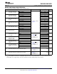
RECOMMENDED OPERATING CONDITIONS
over operating free-air temperature range (unless otherwise noted)
MIN NOM MAX UNIT
V
CC
Supply voltage 4.5 5.5
V
V
I
or V
IC
Voltage at any bus terminal (separately or common mode) –7
(1)
12
SN65HVD50, SN65HVD53 25
1/t
UI
Signaling rate SN65HVD51, SN65HVD54 5 Mbps
SN65HVD52, SN65HVD55 1
R
L
Differential load resistance 54 60 Ω
V
IH
High-level input voltage D, DE, RE 2 V
CC
V
IL
Low-level input voltage D, DE, RE 0 0.8 V
V
ID
Differential input voltage -12 12
Driver -60
I
OH
High-level output current mA
Receiver –8
Driver 60
I
OL
Low-level output current mA
Receiver 8
T
J
(2)
Junction temperature –40 150 °C
(1) The algebraic convention, in which the least positive (most negative) limit is designated as minimum is used in this data sheet.
(2) See thermal characteristics table for information regarding this specification.
ELECTROSTATIC DISCHARGE PROTECTION
PARAMETER TEST CONDITIONS MIN TYP
(1)
MAX UNIT
Human body model Bus terminals and GND ±16
Human body model
(2)
All pins ±4 kV
Charged-device-model
(3)
All pins ±1
(1) All typical values at 25°C and with a 5-V supply.
(2) Tested in accordance with JEDEC Standard 22, Test Method A114-A.
(3) Tested in accordance with JEDEC Standard 22, Test Method C101.
Copyright © 2005–2009, Texas Instruments Incorporated Submit Documentation Feedback 3
Product Folder Link(s) :SN65HVD50-SN65HVD55