
Datasheet


SN65HVD30 – SN65HVD35
www.ti.com
SLLS665I –SEPTEMBER 2005–REVISED APRIL 2010
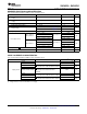
AVAILABLE OPTIONS
BASE
SIGNALING RATE UNIT LOADS ENABLES SOIC MARKING
PART NUMBER
26 Mbps 1/2 No SN65HVD30 VP30
5 Mbps 1/8 No SN65HVD31 VP31
1 Mbps 1/8 No SN65HVD32 VP32
26 Mbps 1/2 Yes SN65HVD33 65HVD33
5 Mbps 1/8 Yes SN65HVD34 65HVD34
1 Mbps 1/8 Yes SN65HVD35 65HVD35
ABSOLUTE MAXIMUM RATINGS
over operating free-air temperature range unless otherwise noted
(1) (2)
UNIT
V
CC
Supply voltage range –0.3 V to 6 V
V
(A)
, V
(B)
, V
(Y)
, V
(Z)
Voltage range at any bus terminal (A, B, Y, Z) –9 V to 14 V
V
(TRANS)
Voltage input, transient pulse through 100 Ω. See Figure 12 (A, B, Y, Z)
(3)
–50 to 50 V
V
I
Input voltage range (D, DE, RE) -0.5 V to 7 V
I
O
Output current (receiver output only, R) 11 mA
(1) Stresses beyond those listed under absolute maximum ratings may cause permanent damage to the device. These are stress ratings
only, and functional operation of the device at these or any other conditions beyond those indicated under recommended operating
conditions is not implied. Exposure to absolute-maximum-rated conditions for extended periods may affect device reliability.
(2) All voltage values, except differential I/O bus voltages, are with respect to network ground terminal.
(3) This tests survivability only and the output state of the receiver is not specified.
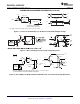
DISSIPATION RATINGS
JEDEC THERMAL T
A
< 25°C DERATING FACTOR T
A
= 85°C T
A
= 105°C T
A
= 125°C
PACKAGE
ABOVE T
A
= 25°C RATING RATING RATING
MODEL RATING
Low k 625 mW 5 mW/°C 325 mW
SOIC (D) 8 pin
High k 1000 mW 8 mW/°C 520 mW 360 mW
Low k 765 mW 6.1 mW/°C 400 mW 275 mW
SOIC (D) 14 pin
High k 1350 mW 10.8 mW/°C 705 mW 485 mW 270 mW
QFN (RHL) 20 pin High k 1710 mW 13.7 mW/°C 890 mW 6150 mW 340 mW
Copyright © 2005–2010, Texas Instruments Incorporated Submit Documentation Feedback 3
Product Folder Link(s) :SN65HVD30 – SN65HVD35