
Datasheet


SN65HVD1780
SN65HVD1781
SN65HVD1782
SLLS877F –DECEMBER 2007–REVISED FEBRUARY 2010
www.ti.com
THERMAL INFORMATION
PARAMETER TEST CONDITIONS VALUE UNIT
JEDEC high-K model 138
SOIC-8
JEDIC low-K model 242
R
qJA
Junction-to-ambient thermal resistance (no airflow) °C/W
JEDEC high-K model 59
DIP-8
JEDIC low-K model 128
SOIC-8 62
R
qJB
Junction-to-board thermal resistance °C/W
DIP-8 39
SOIC-8 61
R
qJC
Junction-to-case thermal resistamce °C/W
DIP-8 61
V
CC
= 3.6V, T
J
= 150°C, R
L
= 300 Ω,
C
L
= 50 pF (driver), C
L
= 15 pF (receiver) 75
3.3-V supply, unterminated
(1)
V
CC
= 3.6V, T
J
= 150°C, R
L
= 100 Ω,
C
L
= 50 pF (driver), C
L
= 15 pF (receiver) 95
3.3-V supply, RS-422 load
(1)
V
CC
= 3.6V, T
J
= 150°C, R
L
= 54 Ω,
C
L
= 50 pF (driver), C
L
= 15 pF (receiver) 115
3.3-V supply, RS-485 load
(1)
P
D
Power dissipation mW
V
CC
= 5.5V, T
J
= 150°C, R
L
= 300 Ω,
C
L
= 50 pF (driver), C
L
= 15 pF (receiver) 290
5-V supply, unterminated
(1)
V
CC
= 5.5V, T
J
= 150°C, R
L
= 100 Ω,
C
L
= 50 pF (driver), C
L
= 15 pF (receiver) 320
5-V supply, RS-422 load
(1)
V
CC
= 5.5V, T
J
= 150°C, R
L
= 54 Ω,
C
L
= 50 pF (driver), C
L
= 15 pF (receiver) 400
5-V supply, RS-485 load
(1)
T
SD
Thermal-shutdown junction temperature 170 °C
(1) Driver and receiver enabled, 50% duty cycle square-wave signal at signaling rate: 1 Mbps.
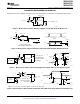
APPLICATION INFORMATION
Hot-Plugging
These devices are designed to operate in "hot swap" or "hot pluggable" applications. Key features for
hot-pluggable applications are power-up, power-down glitch free operation, default disabled input/output pins,
and receiver failsafe. As shown in Figure 9, an internal Power-On Reset circuit keeps the driver outputs in a
high-impedance state until the supply voltage has reached a level at which the device will reliably operate. This
ensures that no problems will occur on the bus pin outputs as the power supply turns on or turns off.
As shown in the device FUNCTION TABLE, the enable inputs have the feature of default disable on both the
driver enable and receiver enable. This ensures that the device will neither drive the bus nor report data on the R
pin until the associated controller actively drives the enable pins.
Receiver Failsafe
The differential receiver is "failsafe" to invalid bus states caused by open bus conditions such as, a disconnected
connector, shorted bus conditions caused by damaged cabling, or idle bus conditions that occur when no driver
is actively driving a valid RD-485 bus state on the network. In any of these cases, the differential receiver will
output a failsafe HIGH state, so that small noise signals do not cause problems at the receiver output.
6 Submit Documentation Feedback Copyright © 2007–2010, Texas Instruments Incorporated
Product Folder Link(s): SN65HVD1780 SN65HVD1781 SN65HVD1782