
Datasheet

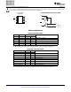


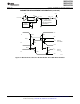


R
RE
DE
D
V
CC
B
A
GND
1
2
3
4
8
7
6
5
S0299-02
1
2
3
4
6
7
A
B
R
RE
DE
D
Bus
SN65HVD1780
SN65HVD1781
SN65HVD1782
SLLS877F –DECEMBER 2007–REVISED FEBRUARY 2010
www.ti.com
These devices have limited built-in ESD protection. The leads should be shorted together or the device placed in conductive foam
during storage or handling to prevent electrostatic damage to the MOS gates.
D or P Package
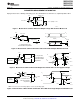
LOGIC DIAGRAM (POSITIVE LOGIC)
(Top View)
DEVICE INFORMATION
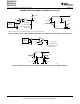
DRIVER FUNCTION TABLE
Input Enable Outputs Driver State
D DE A B
H H H L Actively drive bus High
L H L H Actively drive bus Low
X L Z Z Driver disabled
(1)
X OPEN Z Z Driver disabled by default
(1)
OPEN H H L Actively drive bus High by default
(1) When both the driver and receiver are disabled, the device enters a low-power standby mode.
RECEIVER FUNCTION TABLE
Differential Input Enable Output Receiver State
V
ID
= V
A
– V
B
RE R
V
IT+
< V
ID
L H Receive valid bus High
V
IT–
< V
ID
< V
IT+
L ? Indeterminate bus state
V
ID
< V
IT–
L L Receive valid bus Low
X H Z Receiver disabled
(1)
X OPEN Z Receiver disabled by default
(1)
Open-circuit bus L H Fail-safe high output
Short-circuit bus L H Fail-safe high output
Idle (terminated) bus L H Fail-safe high output
(1) When both the driver and receiver are disabled, the device enters a low-power standby mode.
2 Submit Documentation Feedback Copyright © 2007–2010, Texas Instruments Incorporated
Product Folder Link(s): SN65HVD1780 SN65HVD1781 SN65HVD1782