
Datasheet


Driver Input
Driver Output
Receiver Input
Receiver Output
R
T
R
T
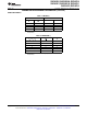
Device
HVD10
HVD11
HVD12
Number of Devices on Bus
64
256
256
NOTE
:
The line should be terminated at both ends with its characteristic impedance (R
T
= Z
O
). Stub lengths off the main line
should be kept as short as possible.
Stub
SN65HVD10, SN65HVD10Q, SN75HVD10
SN65HVD11, SN65HVD11Q, SN75HVD11
SN65HVD12, SN75HVD12
SLLS505M –FEBRUARY 2002–REVISED JULY 2013
www.ti.com
APPLICATION INFORMATION
Figure 23. Typical Application Circuit
Figure 24. HVD12 Input and Output Through 2000 Feet of Cable
An example application for the HVD12 is illustrated in Figure 23. Two HVD12 transceivers are used to
communicate data through a 2000 foot (600 m) length of Commscope 5524 category 5e+ twisted pair cable. The
bus is terminated at each end by a 100- Ω resistor, matching the cable characteristic impedance. Figure 24
illustrates operation at a signaling rate of 250 kbps.
LOW-POWER STANDBY MODE
When both the driver and receiver are disabled (DE low and RE high) the device is in standby mode. If the
enable inputs are in this state for less than 60 ns, the device does not enter standby mode. This guards against
inadvertently entering standby mode during driver/receiver enabling. Only when the enable inputs are held in this
state for 300 ns or more, the device is assured to be in standby mode. In this low-power standby mode, most
internal circuitry is powered down, and the supply current is typically less than 1 nA. When either the driver or the
receiver is re-enabled, the internal circuitry becomes active.
16 Submit Documentation Feedback Copyright © 2002–2013, Texas Instruments Incorporated
Product Folder Links: SN65HVD10 SN65HVD10Q SN75HVD10 SN65HVD11 SN65HVD11Q SN75HVD11
SN65HVD12 SN75HVD12