
Datasheet


DRIVER SECTION
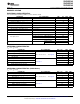
ELECTRICAL CHARACTERISTICS
SWITCHING CHARACTERISTICS
SWITCHING CHARACTERISTICS (SN55LBC180)
SN55LBC180
SN65LBC180
SN75LBC180
SLLS174G – FEBRUARY 1994 – REVISED APRIL 2009 ...................................................................................................................................................
www.ti.com
over recommended operating conditions (unless otherwise noted)
PARAMETER TEST CONDITIONS MIN TYP
(1)
MAX UNIT
V
IK
Input clamp voltage I
I
= -18 mA – 1.5 V
SN55LBC180 1 2.5 5
R
L
= 54 Ω ,
SN65LBC180 1.1 2.5 5
See Figure 1
SN75LBC180 1.5 2.5 5
| V
OD
| Differential output voltage magnitude
(2)
V
SN55LBC180 1 2.5 5
R
L
= 60 Ω ,
SN65LBC180 1.1 2 5
See Figure 2
SN75LBC180 1.5 2 5
Δ | V
OD
| Change in magnitude of differential output voltage
(3)
See Figure 1 and Figure 2 ± 0.2 V
V
OC
Common-mode output voltage 1 2.5 3 V
R
L
= 54 Ω , See Figure 1
Change in magnitude of common-mode output
Δ | V
OC
| ± 0.2 V
voltage
(3)
I
O
Output current with power off V
CC
= 0, V
O
= – 7 V to 12 V ± 100 µ A
I
OZ
High-impedance-state output current V
O
= – 7 V to 12 V ± 100 µ A
I
IH
High-level input current V
I
= 2.4 V 100 µ A
I
IL
Low-level input current V
I
= 0.4 V 100 µ A
I
OS
Short-circuit output current – 7 V ≤ V
O
≤ 12 V ± 250 mA
Outputs enabled 5
I
CC
Supply current Receiver disabled mA
Outputs disabled 3
(1) All typical values are at V
CC
= 5 V and T
A
= 25 ° C.
(2) The minimum V
OD
specification may not fully comply with ANSI RS-485 at operating temperatures below 0 ° C. System designers should
take the possibly lower output signal into account in determining the maximum signal-transmission distance.
(3) Δ |V
OD
| and Δ |V
OC
| are the changes in the steady-state magnitude of V
OD
and V
OC
, respectively, that occur when the input is changed
from a high level to a low level.
V
CC
= 5 V, T
A
= 25 ° C
PARAMETER TEST CONDITIONS MIN TYP MAX UNIT
t
d(OD)
Differential output delay time 7 12 18 ns
R
L
= 54 Ω , See Figure 3
t
t(OD)
Differential output transition time 5 10 20 ns
t
PZH
Output enable time to high level R
L
= 110 Ω , See Figure 4 35 ns
t
PZL
Output enable time to low level R
L
= 110 Ω , See Figure 5 35 ns
t
PHZ
Output disable time from high level R
L
= 110 Ω , See Figure 4 50 ns
t
PLZ
Output disable time from low level R
L
= 110 Ω , See Figure 5 35 ns
V
CC
= 5 V, T
A
= 25 ° C
PARAMETER TEST CONDITIONS MIN TYP MAX UNIT
t
d(OD)
Differential output delay time 15 ns
R
L
= 54 Ω , See Figure 3
t
t(OD)
Differential output transition time 21 ns
t
PZH
Output enable time to high level 32
R
L
= 110 Ω , See Figure 4 ns
t
PHZ
Output disable time from high level 55
t
PZL
Output enable time to low level 32
R
L
= 110 Ω , See Figure 5 ns
t
PLZ
Output disable time from low level 20
4 Submit Documentation Feedback Copyright © 1994 – 2009, Texas Instruments Incorporated
Product Folder Link(s): SN55LBC180 SN65LBC180 SN75LBC180