
Datasheet


SM73308
www.ti.com
SNOSB90B –JUNE 2011–REVISED APRIL 2013
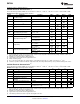
2.7V DC Electrical Characteristics
(1)
Unless otherwise specified, all limits are ensured for T
A
= 25°C. V
+
= 2.7V, V
−
= 0V, V
CM
= V
+
/2, V
O
= V
+
/2 and R
L
> 1MΩ.
Boldface limits apply at the temperature extremes.
Symbol Parameter Condition Min
(2)
Typ
(3)
Max
(2)
Units
0.3 0.85
V
OS
Input Offset Voltage mV
1.0
TCV
OS
Input Offset Voltage Average Drift −0.45 µV/°C
−0.1 100
I
B
Input Bias Current
(4)
V
CM
= 1V pA
250
I
OS
Input Offset Current
(4)
0.004 100 pA
550 900
I
S
Supply Current µA
910
74 80
CMRR Common Mode Rejection Ratio 0.5 ≤ V
CM
≤ 1.2V dB
72
82 90 dB
PSSR Power Supply Rejection Ratio 2.7V ≤ V
+
≤ 5V
76
V
CM
Input Common-Mode Voltage Range For CMRR ≥ 50dB 0 1.8 V
R
L
= 600Ω to 1.35V, 92 100
V
O
= 0.2V to 2.5V 80
A
V
Large Signal Voltage Gain
(5)
dB
R
L
= 2kΩ to 1.35V, 98 100
V
O
= 0.2V to 2.5V 86
R
L
= 600Ω to 1.35V 0.11 0.084 to 2.59
V
IN
= ± 100mV 0.14 2.62 2.56
V
O
Output Swing V
R
L
= 2kΩ to 1.35V 0.05 0.026 to 2.65
V
IN
= ± 100mV 0.06 2.68 2.64
Sourcing, V
O
= 0V 18 24
V
IN
= 100mV 11
I
O
Output Short Circuit Current mA
Sinking, V
O
= 2.7V 18 22
V
IN
= −100mV 11
(1) Electrical Table values apply only for factory testing conditions at the temperature indicated. Factory testing conditions result in very
limited self-heating of the device such that T
J
= T
A
.
(2) All limits are ensured by testing or statistical analysis.
(3) Typical values represent the most likely parametric norm.
(4) Limits ensured by design.
(5) R
L
is connected to mid-supply. The output voltage is set at 200mV from the rails. V
O
= GND + 0.2V and V
O
= V
+
−0.2V
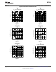
2.7V AC Electrical Characteristics
(1)
Unless otherwise specified, all limits are ensured for T
A
= 25°C. V
+
= 5.0V, V
−
= 0V, V
CM
= V
+
/2, V
O
= V
+
/2 and R
L
> 1MΩ.
Boldface limits apply at the temperature extremes.
Symbol Parameter Conditions Min
(2)
Typ
(3)
Max
(2)
Units
SR Slew Rate
(4)
A
V
= +1, R
L
= 10 kΩ 1.4 V/µs
GBW Gain-Bandwidth Product 3.5 MHz
Φ
m
Phase Margin 79 Deg
G
m
Gain Margin −15 dB
Input-Referred Voltage Noise
e
n
f = 10kHz 7.5 nV/√Hz
(Flatband)
e
n
Input-Referred Voltage Noise (l/f) f = 100Hz 12.5 nV/√Hz
i
n
Input-Referred Current Noise f = 1kHz 0.001 pA/√Hz
f = 1kHz, A
V
= +1
THD Total Harmonic Distortion 0.007 %
R
L
= 600Ω, V
IN
= 1 V
PP
(1) Electrical Table values apply only for factory testing conditions at the temperature indicated. Factory testing conditions result in very
limited self-heating of the device such that T
J
= T
A
.
(2) All limits are ensured by testing or statistical analysis.
(3) Typical values represent the most likely parametric norm.
(4) The number specified is the slower of positive and negative slew rates.
Copyright © 2011–2013, Texas Instruments Incorporated Submit Documentation Feedback 3
Product Folder Links: SM73308