
Datasheet


REG102
10
SBVS024F
www.ti.com
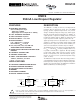
FIGURE 4. Block Diagram.
FIGURE 5. Output Noise versus Noise Reduction Capacitor.
0.1 100 1k10 10k
110
100
90
80
70
60
50
40
30
20
Noise Voltage (Vrms)
C
NR
(pF)
RMS NOISE VOLTAGE vs C
NR
REG102-5.0
REG102-3.3
REG102-2.5
C
OUT
= 0µF
10Hz < BW < 100kHz
Over-Current
Over Temp
Protection
V
REF
(1.26V)
Low-Noise
Charge Pump
DMOS
Output
R
1
NOTE: R
1
and R
2
are internal
on fixed output versions.
V
OUT
Adj
(adjustable
versions)
R
2
NR
(fixed output
versions only)
Enable
REG102
V
IN
C
NR
(optional)
ENABLE
The Enable pin is active high and compatible with standard
TTL-CMOS levels. Inputs below 0.5V (max) turn the regula-
tor off and all circuitry is disabled. Under this condition,
ground pin current drops to approximately 10nA. When not
used, the Enable pin can be connected to V
IN
. When a pull-
up resistor is used, and operation below 1.8V is required, use
pull-up resistor values below 50kΩ.
OUTPUT NOISE
A precision bandgap reference is used to generate the
internal reference voltage, V
REF
. This reference is the domi-
nant noise source within the REG102 and generates approxi-
mately 29µVrms in the 10Hz to 100kHz bandwidth at the
reference output. The regulator control loop gains up the
reference noise, so that the noise voltage of the regulator is
approximately given by:
V Vrms
RR
R
Vrms
V
V
N
OUT
REF
=µ
+
=µ •29
2
29
12
(1)
As the value of V
REF
is 1.26V, this relationship reduces to:
V
Vrms
V
V
N
OUT
=
µ
•23
(2)
Connecting a capacitor, C
NR
, from the Noise Reduction (NR)
pin to ground forms a low-pass filter for the voltage refer-
ence. Adding C
NR
(as shown in Figure 4) forms a low-pass
filter for the voltage reference. For C
NR
= 10nF, the total noise
in the 10Hz to 100kHz bandwidth is reduced by approxi-
mately a factor of 2.8 for V
OUT
= 3.3V. This noise reduction
effect is shown in Figure 5 and as
RMS Noise Voltage vs C
NR
in the Typical Characteristics section.
Noise can be further reduced by carefully choosing an output
capacitor, C
OUT
. Best overall noise performance is achieved
with very low (< 0.22µF) or very high (> 2.2µF) values of C
OUT
(see the
RMS Noise Voltage vs C
OUT
typical characteristic).
The REG102 uses an internal charge pump to develop an
internal supply voltage sufficient to drive the gate of the
DMOS pass element above V
IN
. The charge-pump switching
noise (nominal switching frequency = 2MHz) is not measur-
able at the output of the regulator over most values of I
OUT
and C
OUT
.
The REG102 adjustable version does not have the noise-
reduction pin available; however, the adjust pin is the sum-
ming junction of the error amplifier. A capacitor, C
FB
, con-
nected from the output to the adjust pin can reduce both the
output noise and the peak error from a load transient (see the
typical characteristics for output noise performance).