
Datasheet


www.ti.com
POWER DISSIPATION APPLICATION CIRCUITS
T =T +P ´ q
J A D JA
(2)
NOISE PERFORMANCE
R
3
R
2
V
IN
+2.7V
Enable
(1)
OPA333,
OPA363,
OPA369
or
R
66.5
1
W
C
1.5nF
1
C
1 F
2
m
P1.2
VREF
A0+
REF3312
+2.7V
V
CC
V
SS
16-Bit
ADC
MSP430x20x3PW
REF3312 , , REF3318
REF3320 , REF3325
REF3330 , REF3333
SBOS392A – AUGUST 2007 – REVISED SEPTEMBER 2007
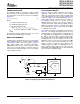
The REF33xx family is specified to deliver current Figure 20 shows a simple application circuit where
loads of ± 5mA over the specified input voltage range. low-power components are used to create a signal
The temperature of the device increases according to chain. The analog input signal is buffered with either
Equation 2 : a zero-drift OPA333 or zero-crossover OPA363 . The
reference voltage created from REF3312 provides a
stable, high-accuracy, low-drift reference voltage to
the MSP430 using much less power than the
Where:
MSP430 internal reference. The reference voltage is
T
J
= Junction temperature ( ° C)
used by the internal, 16-bit analog-to-digital converter
T
A
= Ambient temperature ( ° C)
(ADC) to accurately convert the analog input signal.
P
D
= Power dissipation (W)
The configuration in Figure 20 presents an example
Where P
D
= V
IN
× I
Q
+ (V
IN
– V
OUT
) I
OUT
of a unipolar signal chain.
θ
JA
= Junction-to-ambient thermal resistance
An example of a bipolar configuration is illustrated in
( ° C/W)
Figure 21 . The analog input signal ( ± 2.5V) is offset
and attenuated so that it matches the analog input of
The REF33xx junction temperature must not exceed
the 16-bit ADC on the MSP430. The negative input of
the absolute maximum rating of +150 ° C.
the ADC is offset by 0.62V, creating a digital code
that corresponds to the analog input voltage. In this
configuration, two reference voltages are used. The
Typical 0.1Hz to 10Hz voltage noise for each member
REF3312 creates a 1.25V reference input to the ADC
of the REF33xx family is specified in the Electrical
and is an offset point for the INA159 . The same
Characteristics table. The noise voltage increases
voltage is used to create the offset voltage to the
with output voltage and operating temperature.
negative input to the ADC. The REF3330 creates a
Additional filtering can be used to improve output
precise analog supply voltage of 3V. In this way, the
noise levels. Special attention should be taken to
high PSRR of the REF3330 helps to filter unwanted
ensure that the output impedance does not degrade
noise from the 3.3V digital supply.
output voltage accuracy.
(1) Enable is a function of the OPA363 not available on the OPA333.
Figure 20. Unipolar Signal Chain Configuration
Copyright © 2007, Texas Instruments Incorporated Submit Documentation Feedback 9
Product Folder Link(s): REF3312 REF3318 REF3320 REF3325 REF3330 REF3333