
Datasheet


www.ti.com
APPLICATIONS INFORMATION
SUPPLY VOLTAGE
START-UP TIME
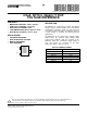
V
IN
REF33xx
GND
V
OUT
1.2V
Bandgap
BASIC CONNECTIONS
REF33xx
V
IN
V
OUT
V
OUT
V
IN
C
BYPASS
1 Fto10 F
(recommended)
m m
C
L
0.1 Fto10 Fm m
GND
1V/div
Time(400 s/div)m
V
IN
0.1 Fm
1 Fm
10 Fm
TEMPERATURE DRIFT
Drift=
V V-
OUTMAX OUTMIN
V TempRange´
OUT
´ 10 (ppm)
6
(1)
REF3312 , , REF3318
REF3320 , REF3325
REF3330 , REF3333
SBOS392A – AUGUST 2007 – REVISED SEPTEMBER 2007
The REF33xx is a family of low-power, precision
bandgap voltage references that are specifically
The REF33xx family of voltage references features
designed for excellent initial voltage accuracy with a
extremely low dropout voltage, except for the
high output current. Figure 17 shows a simplified
REF3312. The REF3312 has a minimum supply
block diagram of the REF33xx.
requirement of 1.8V. These references can be
operated with a supply 110mV above the output
voltage with a 5mA load (typical). For loaded
conditions, a typical dropout voltage versus load
graph is illustrated in Figure 4 of the Typical
Characteristics .
If the supply voltage connected to the IN pin is rapidly
moved while the REF33xx is connected to a
capacitive load, a reverse voltage may discharge
through the OUT pin and into the REF33xx device.
This voltage will not damage the REF33xx, provided
that it is less than or equal to 5V.
The REF33xx features an advanced start-up circuit.
Start-up time is almost independent of load (with a
Figure 17. REF33xx Simplified Block Diagram
0.1 μ F to 10 μ F load). Upon start-up, the current boost
circuit forces the output voltage. When the preset
voltage is reached, the REF33xx switches to the
second stage of output circuitry to precisely set the
output voltage. Figure 19 shows the start-up time of
Figure 18 shows the typical connections for the
the REF3325 for three different capacitive loads. In
REF33xx. A recommended supply bypass capacitor
all three cases, the output voltage settles within 2ms.
ranging between 1 μ F to 10 μ F is recommended. The
total capacitive load at the output must be between
0.1 μ F to 10 μ F to ensure output stability.
Figure 18. Basic Connections
Figure 19. Start-Up Time
The REF33xx is designed for minimal drift error,
defined as the change in output voltage over
temperature. The drift is calculated using the box
method, as described in Equation 1 :
8 Submit Documentation Feedback Copyright © 2007, Texas Instruments Incorporated
Product Folder Link(s): REF3312 REF3318 REF3320 REF3325 REF3330 REF3333