
Datasheet


REF3012, 3020, 3025, 3030, 3033, 3040
8
SBVS032F
www.ti.com
THEORY OF OPERATION
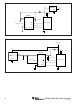
The REF30xx is a series, CMOS, precision bandgap voltage
reference. Its basic topology is shown in Figure 1. The
transistors Q
1
and Q
2
are biased such that the current
density of Q
1
is greater than that of Q
2
. The difference of the
two base-emitter voltages, Vbe
1
– Vbe
2
, has a positive
temperature coefficient and is forced across resistor R
1
. This
voltage is gained up and added to the base-emitter voltage
of Q
2
, which has a negative coefficient. The resulting output
voltage is virtually independent of temperature. The curvature
of the bandgap voltage, as seen in the typical curve, “Output
Voltage vs Temperature,” is due to the slightly nonlinear
temperature coefficient of the base-emitter voltage of Q
2
.
The REF30xx features a low quiescent current, which is
extremely stable over changes in both temperature and
supply. The typical room temperature quiescent current is
42µA, and the maximum quiescent current over temperature
is just 59µA. Additionally, the quiescent current typically
changes less than 2.5µA over the entire supply range, as
shown in Figure 3.
Supply voltages below the specified levels can cause the
REF30xx to momentarily draw currents greater than the
typical quiescent current. Using a power supply with a fast
rising edge and low output impedance easily prevents this.
1
3
REF30xx
2
0.47µF
V
IN
V
OUT
FIGURE 1. Simplified Schematic of Bandgap Reference.
FIGURE 2. Typical Connections for Operating REF30xx.
SUPPLY CURRENT vs INPUT VOLTAGE
42.5
42.0
41.5
41.0
40.5
40.0
I
Q
(µA)
1 1.5 2 2.5 3 3.5 4 4.5 5 5.5 6
V
IN
(V)
FIGURE 3. Supply Current vs Supply Voltage.
R
1
Q
2
Q
1
+
Vbe
1
–
+
Vbe
2
–
APPLICATION INFORMATION
For normal operation, the REF30xx does not require a
capacitor on the output. If a capacitive load is connected,
special care must be taken with the combination of low
equivalent series resistance (ESR) capacitors and high
capacitance. This caution is especially true for low-output
voltage devices; therefore, the REF3012 should only have a
low-ESR capacitance of 10µF or less. Figure 2 shows the
typical connections required for operation of the REF30xx. A
supply bypass capacitor of 0.47µF is always recommended.
SUPPLY VOLTAGE
The REF30xx family of references features an extremely low
dropout voltage. With the exception of the REF3012, which has
a minimum supply requirement of 1.8V, the REF30xx can be
operated with a supply of only 1mV above the output voltage in
an unloaded condition. For loaded conditions, a typical dropout
voltage versus load is shown on the cover page.
THERMAL HYSTERESIS
Thermal hysteresis for the REF30xx is defined as the change
in output voltage after operating the device at 25°C, cycling
the device through the specified temperature range, and
returning to 25°C, and can be expressed as:
V
absV V
V
ppm
HYST
PRE
POST
NOM
=
•
(
)
–
10
6
Where: V
HYST
=
Calculated hysteresis
V
PRE
= Output voltage measured at 25°C pre-
temperature cycling
V
POST
= Output voltage measured when device has
been operated at 25°C, cycled through specified
range –40°C to +125°C and returned to operation at
25°C.
TEMPERATURE DRIFT
The REF30xx is designed to exhibit minimal drift error, defined
as the change in output voltage over varying temperature.
Using the “box” method of drift measurement, the REF30xx
features a typical drift coefficient of 20ppm from 0°C to 70°C—
the primary temperature range of use for many applications.
For industrial temperature ranges of –40°C to 125°C, the
REF30xx family drift increases to a typical value of 50ppm.