
Datasheet


REF102
5
SBVS022B
www.ti.com
TYPICAL CHARACTERISTICS (Cont.)
At T
A
= +25°C, V
S
= +15V, unless otherwise noted.
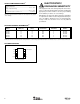
TYPICAL REF102 REFERENCE NOISE
6
4
2
0
−2
−4
−6
Low Frequency Noise (1s/div)
(See Noise Test Circuit)
Noise Voltage (µV)
–
+
OPA227
DUT
Noise Test Circuit.
100µF
15.8kΩ
20Ω 2kΩ
8kΩ
2µF
Oscilloscope
Gain = 100V/V
f = 0.1Hz and 10Hz
−3dB
THEORY OF OPERATION
Refer to the diagram on the first page of this data sheet. The
10V output is derived from a compensated buried zener
diode DZ
1
, op amp A
1
, and resistor network R
1
– R
6
.
Approximately 8.2V is applied to the non-inverting input of A
1
by DZ
1
. R
1
, R
2
, and R
3
are laser-trimmed to produce an exact
10V output. The zener bias current is established from the
regulated output voltage through R
4
. R
5
allows user-trimming
of the output voltage by providing for small external adjust-
ment of the amplifier gain. Because the temperature coeffi-
cient (TCR) of of R
5
closely matches the TCR of R
1
, R
2
and
R
3
, the voltage trim has minimal effect on the reference drift.
The output voltage noise of the REF102 is dominated by the
noise of the zener diode. A capacitor can be connected
between the Noise Reduction pin and ground to form a low-
pass filter with R
6
and roll off the high-frequency noise of the
zener.
DISCUSSION
OF PERFORMANCE
The REF102 is designed for applications requiring a preci-
sion voltage reference where both the initial value at room
temperature and the drift over temperature are of importance
to the user. Two basic methods of specifying voltage refer-
ence drift versus temperature are in common usage in the
industry—the
butterfly method
and the
box method
. The
REF102 is specified by the more commonly-used
box method.
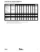
The
box
is formed by the high and low specification tempera-
tures and a diagonal, the slope of which is equal to the
maximum specified drift.
Since the shape of the actual drift curve is not known, the
vertical position of the box is not known, either. It is, however,
bounded by V
UPPER BOUND
and V
LOWER BOUND
(see Figure 1).
Figure 1 uses the REF102CU as an example. It has a drift
specification of 2.5ppm/°C maximum and a specification
temperature range of –25°C to +85°C. The
box
height,
V
1
to V
2
, is 2.75mV.
REF102CU V
UPPER BOUND
+10.00275
V
1
V
NOMINAL
+10.0000
2.75mV
Worst-case
∆V
OUT
for
REF102CU
V
2
+9.99725
REF102CU V
LOWER BOUND
−25 0 +25 +50 +85
Output Voltage (V)
Temperature (°C)
FIGURE 1. REF102CU Output Voltage Drift.