
Datasheet


REF02
3
SBVS003B
www.ti.com
Input Voltage ..................................................................................... +40V
Operating Temperature
P, U ................................................................................ –40°C to +85°C
Storage Temperature Range
P, U ................................................................................ –65°C to +125°
Output Short Circuit Duration (to Ground or V
IN
) ........................ Indefinite
Junction Temperature ....................................................... –65°C to +150°
θ
JA
P ......................................................................................... 120°C/W
U ........................................................................................... 80°C/W
Lead Temperature (soldering, 60s) ............................................... +300°C
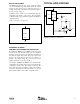
ABSOLUTE MAXIMUM RATINGS PIN CONFIGURATIONS
Top View DIP/SO
NC
V
IN
Temp
GND
NC
NC
V
OUT
Trim
1
2
3
4
8
7
6
5
ELECTROSTATIC
DISCHARGE SENSITIVITY
This integrated circuit can be damaged by ESD. Texas Instru-
ments recommends that all integrated circuits be handled with
appropriate precautions. Failure to observe proper handling
and installation procedures can cause damage.
ESD damage can range from subtle performance degradation
to complete device failure. Precision integrated circuits may
be more susceptible to damage because very small parametric
changes could cause the device not to meet its published
specifications.
PACKAGE/ORDERING INFORMATION
(1)
PACKAGE SPECIFICATION
MAX DRIFT DRAWING TEMPERATURE
PRODUCT V
OUT
at 25°C (ppm/°C) PACKAGE DESIGNATOR RANGE
REF02AU 5V±15mV ±15 SO-8 D –40°C to +85°C
REF02BU 5V±10mV ±10 SO-8 D –40°C to +85°C
REF02AP 5V±15mV ±15 DIP-8 P –40°C to +85°C
REF02BP 5V±10mV ±10 DIP-8 P –40°C to +85°C
NOTE: (1) For the most current package and ordering information, see the Package Option Addendum located at the end of this data sheet, or see the TI website
at www.ti.com.