
Datasheet


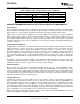

DEVICE INFORMATION
PTHXX060
(Top View)
1
2
10 9 8
7
6
543
PTH12060W/L
www.ti.com
.................................................................................................................................................... SLTS217H – MAY 2003 – REVISED DECEMBER 2008
Terminal Functions
TERMINAL
DESCRIPTION
NAME NO.
V
I
2 The positive input voltage power node to the module, which is referenced to common GND.
V
O
6 The regulated positive power output with respect to the GND node.
This is the common ground connection for the V
I
and V
O
power connections. It is also the 0 Vdc reference for the
GND 1, 7
control inputs.
The Inhibit pin is an open-collector/drain negative logic input that is referenced to GND. Applying a low level ground
signal to this input disables the module ’ s output and turns off the output voltage. When the Inhibit control is active,
the input current drawn by the regulator is significantly reduced. If the Inhibit pin is left open-circuit, the module
Inhibit 3
produces an output whenever a valid input source is applied. Do not place an external pull-up on this pin. For
power-up into a non-prebiased output, it is recommended that AutoTrack be utilized for On/Off control. See the
Application Information for additional details.
A 1% resistor must be directly connected between this pin and GND (pin 1) to set the output voltage of the module
to a value higher than its lowest value. The temperature stability of the resistor should be 100 ppm/ ° C (or better).
The set-point range is 1.2 V to 5.5 V for W-suffix devices, and 0.8 V to 1.8 V for L-suffix devices. The resistor value
V
O
Adjust 4
required for a given output voltage may be calculated using a formula. If left open circuit, the output voltage defaults
to its lowest value. For further information on output voltage adjustment, see the application information section.
Table 2 gives the preferred resistor values for a number of standard output voltages.
The sense input allows the regulation circuit to compensate for voltage drop between the module and the load. For
V
O
Sense 5
optimal voltage accuracy, V
O
Sense should be connected to V
O
. It can also be left disconnected.
This is an analog control input that enables the output voltage to follow an external voltage. This pin becomes
active typically 20 ms after the input voltage has been applied, and allows direct control of the output voltage from
zero volts, up to the nominal set-point voltage. Within this range, the output follows the voltage at the Track pin on a
Track 8
volt-for-volt basis. When the control voltage is raised above this range, the module regulates at its set-point voltage.
The feature allows the output voltage to rise simultaneously with other modules powered from the same input bus.
If unused, this input should be connected to V
I
.
Note: Due to the undervoltage lockout feature, the output of the module cannot follow its own input voltage during
power up. For more information, see the application information section.
When this input is asserted to GND, the output voltage is decreased by 5% from the nominal. The input requires an
Margin Down 9 open-collector (open-drain) interface. It is not TTL compatible. A lower percent change can be accommodated with
a series resistor. For further information, see the application information section.
When this input is asserted to GND, the output voltage is increased by 5%. The input requires an open-collector
Margin Up 10 (open-drain) interface. It is not TTL compatible. The percent change can be reduced with a series resistor. For
further information, see the application information section.
Copyright © 2003 – 2008, Texas Instruments Incorporated Submit Documentation Feedback 5
Product Folder Link(s): PTH12060W/L