
Datasheet


12PGA204/205
®
it to its highest gain and trimming the output voltage to zero
with the inputs grounded. Drift performance usually im-
proves slightly when the input offset is nulled with this
procedure.
Do not use the input offset adjustment to trim system offset
or offset produced by a sensor. Nulling offset that is not
produced by the input amplifiers will increase temperature
drift by approximately 3.3µV/°C per 1mV of offset adjust-
ment.
Many applications that need input stage offset adjustment do
not need output stage offset adjustment. Figure 3 also shows
a circuit for adjusting output offset voltage. First, adjust the
input offset voltage as discussed above. Then program the
device for G=1 and adjust the output to zero. Because of the
interaction of these two adjustments at G=8, the PGA205
may require iterative adjustment.
The output offset adjustment can be used to trim sensor or
system offsets without affecting drift. The voltage applied to
the Ref terminal is summed with the output signal. Low
impedance must be maintained at this node to assure good
common-mode rejection. This is achieved by buffering the
trim voltage with an op amp as shown.
NOISE PERFORMANCE
The PGA204/205 provides very low noise in most applica-
tions. Low frequency noise is approximately 0.4µVp-p mea-
sured from 0.1 to 10Hz. This is approximately one-tenth the
noise of “low noise” chopper-stabilized amplifiers.
INPUT BIAS CURRENT RETURN PATH
The input impedance of the PGA204/205 is extremely high—
approximately 10
10
Ω. However, a path must be provided for
the input bias current of both inputs. This input bias current
is typically less than ±1nA (it can be either polarity due to
cancellation circuitry). High input impedance means that
this input bias current changes very little with varying input
voltage.
Input circuitry must provide a path for this input bias current
if the PGA204/205 is to operate properly. Figure 4 shows
provisions for an input bias current path. Without a bias
current return path, the inputs will float to a potential which
exceeds the common-mode range of the PGA204/205 and
the input amplifiers will saturate. If the differential source
resistance is low, bias current return path can be connected
to one input (see thermocouple example in Figure 4). With
higher source impedance, using two resistors provides a
balanced input with possible advantages of lower input
offset voltage due bias current and better common-mode
rejection.
Many sources or sensors inherently provide a path for input
bias current (e.g. the bridge sensor shown in Figure 4).
These applications do not require additional resistor(s) for
proper operation.
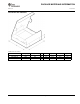
FIGURE 4. Providing an Input Common-Mode Current
Path.
INPUT COMMON-MODE RANGE
The linear common-mode range of the input op amps of the
PGA204/205 is approximately ±12.7V (or 2.3V from the
power supplies). As the output voltage increases, however,
the linear input range will be limited by the output voltage
swing of the input amplifiers, A
1
and A
2
. The common-
mode range is related to the output voltage of the complete
amplifier—see performance curve “Input Common-Mode
Range vs Output Voltage”.
A combination of common-mode and differential input
voltage can cause the output of A
1
or A
2
to saturate. Figure
5 shows the output voltage swing of A
1
and A
2
expressed in
terms of a common-mode and differential input voltages.
Output swing capability of these internal amplifiers is the
same as the output amplifier, A
3
. For applications where
input common-mode range must be maximized, limit the
output voltage swing by selecting a lower gain of the
PGA204/205 (see performance curve “Input Common-Mode
Voltage Range vs Output Voltage”). If necessary, add gain
after the PGA204/205 to increase the voltage swing.
47kΩ47kΩ
10kΩ
Microphone,
Hydrophone
etc.
Thermocouple
Center-tap provides
bias current return.
V
R
Bridge
Bias current return
inherrently provided by source.
PGA204
PGA204
PGA204
PGA204