
Datasheet


PCM5100, PCM5101, PCM5102
www.ti.com
SLAS764B –MAY 2011–REVISED SEPTEMBER 2012
This integrated circuit can be damaged by ESD. Texas Instruments recommends that all integrated circuits be handled with
appropriate precautions. Failure to observe proper handling and installation procedures can cause damage.
ESD damage can range from subtle performance degradation to complete device failure. Precision integrated circuits may be more
susceptible to damage because very small parametric changes could cause the device not to meet its published specifications.
DEVICE INFORMATION
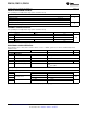
TERMINAL FUNCTIONS, PCM510x
PCM510x (top view)
Table 2. TERMINAL FUNCTIONS, PCM510x
TERMINAL
I/O DESCRIPTION
NAME NO.
CPVDD 1 — Charge pump power supply, 3.3V
CAPP 2 O Charge pump flying capacitor terminal for positive rail
CPGND 3 — Charge pump ground
CAPM 4 O Charge pump flying capacitor terminal for negative rail
VNEG 5 O Negative charge pump rail terminal for decoupling, -3.3V
OUTL 6 O Analog output from DAC left channel
OUTR 7 O Analog output from DAC right channel
AVDD 8 -— Analog power supply, 3.3V
AGND 9 — Analog ground
DEMP 10 I De-emphasis control for 44.1kHz sampling rate
(1)
: Off (Low) / On (High)
FLT 11 I Filter select : Normal latency (Low) / Low latency (High)
SCK 12 I System clock input
(1)
BCK 13 I Audio data bit clock input
(1)
DIN 14 I Audio data input
(1)
LRCK 15 I Audio data word clock input
(1)
FMT 16 I Audio format selection : I
2
S (Low) / Left justified (High)
XSMT 17 I Soft mute control
(1)
: Soft mute (Low) / soft un-mute (High)
LDOO 18 — Internal logic supply rail terminal for decoupling
DGND 19 — Digital ground
DVDD 20 — Digital power supply, 3.3V
(1) Failsafe LVCMOS Schmitt trigger input
Copyright © 2011–2012, Texas Instruments Incorporated Submit Documentation Feedback 3
Product Folder Links: PCM5100 PCM5101 PCM5102