
Datasheet


www.ti.com
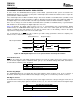
BOARD DESIGN AND LAYOUT CONSIDERATIONS
V
CC
, V
DD
Pins
AGND, DGND Pins
V
IN
L[1:6], V
IN
R[1:6] Pins
MOUTL, MOUTR Pins
V
REF
1, V
REF
2, V
REF
S Pins
BCK and LRCK Pins (in Master Mode), DOUT Pin
System Clock
PCM1850A
PCM1851A
SLES173 – MARCH 2006
APPLICATION INFORMATION (continued)
The digital and analog power supply lines to the PCM1850A/1851A must be bypassed to the corresponding
ground pins with 0.1- µ F ceramic and 10- µ F electrolytic capacitors as close to the pins as possible to maximize
the dynamic performance of the ADC.
To maximize the dynamic performance of the PCM1850A/1851A, the analog and digital grounds are not
connected internally. These grounds must have low impedance to avoid digital noise feeding back into the
analog ground. Therefore, they should be connected directly to each other under the parts to reduce the potential
of a noise problem.
A 0.33- µ F capacitor is recommended as the ac-coupling capacitor, which gives a 2.4- to 8.5-Hz cutoff frequency.
If higher full-scale input voltage is required, it can be adjusted by adding only one series resistor to each V
IN
xx
pin, but a signal source resistance less than 1 k Ω is recommended for these pins in order to keep accuracy of
the gain control command and to maintain crosstalk performance.
An ac-coupled light load is recommended; a 2.2- µ F capacitor with a 10-k Ω load gives a 7.2-Hz cutoff frequency.
Between V
REF
1 and AGND, V
REF
2 and AGND, and V
REF
S and AGND, 0.1- µ F ceramic and 10- µ F electrolytic
capacitors are recommended to ensure low source impedance of the ADC references. These capacitors should
be located as close as possible to the V
REF
1, V
REF
2, and V
REF
S pins to reduce dynamic errors on the ADC
references. The differential voltage between V
REF
2 and AGND sets the analog input full-scale range.
These pins have enough load-driving capability. However, if the output line is long, locating a buffer near the
PCM1850A/1851A and minimizing load capacitance is recommended in order to minimize the digital-analog
crosstalk and maximize the dynamic performance of the ADC.
Because the PCM1850A/1851A operates based on a system clock, the quality of the system clock can influence
dynamic performance. Therefore, it is recommended to consider the system clock duty, jitter, and the time
difference between the system clock transition and the BCK or LRCK transition in slave mode.
29
Submit Documentation Feedback