
Datasheet


www.ti.com
DEVICE INFORMATION
SYSTEM CLOCK
SCKI
0.8 V
SCKI
2 V
t
w(SCKL)
t
w(SCKH)
T0005B07
POWER-ON-RESET SEQUENCE
PCM1803A
SLES142A – JUNE 2005 – REVISED AUGUST 2006
The PCM1803A supports 256 f
S
, 384 f
S
, 512 f
S
, and 768 f
S
as the system clock, where f
S
is the audio sampling
frequency. The system clock must be supplied on SCKI (pin 15).
The PCM1803A has a system clock-detection circuit that automatically senses if the system clock is operating at
256 f
S
, 384 f
S
, 512 f
S
, or 768 f
S
in slave mode. In master mode, the system clock frequency must be selected by
MODE0 (pin 19) and MODE1 (pin 20), and 768 f
S
is not available. The system clock is divided automatically into
128 f
S
and 64 f
S
, and these frequencies are used to operate the digital filter and the delta-sigma modulator.
Table 1 shows the relationship of typical sampling frequency and system clock frequency, and Figure 17 shows
system clock timing.
Table 1. Sampling Frequency and System Clock Frequency
SYSTEM CLOCK FREQUENCY (MHz)
SAMPLING FREQUENCY (kHz)
256 f
S
384 f
S
512 f
S
768 f
S
(1)
32 8.1920 12.2880 16.3840 24.5760
44.1 11.2896 16.9344 22.5792 33.8688
48 12.2880 18.4320 24.5760 36.8640
64 16.3840 24.5760 32.7680 49.1520
88.2 22.5792 33.8688 45.1584 –
96 24.5760 36.8640 49.1520 –
(1) Slave mode only
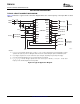
SYMBOL PARAMETER MIN MAX UNIT
t
w(SCKH)
System clock pulse duration, HIGH 8 ns
t
w(SCKL)
System clock pulse duration, LOW 8 ns
Figure 17. System Clock Timing
The PCM1803A has an internal power-on-reset circuit, and initialization (reset) is performed automatically at the
time when power-supply voltage (V
DD
) exceeds 2.2 V (typical). While V
DD
< 2.2 V (typical) and for 1024 system
clock cycles after V
DD
> 2.2 V (typical), the PCM1803A stays in the reset state, and the digital output is forced to
zero. The digital output becomes valid when a time period of 4480/f
S
has elapsed following release from the
reset state. Figure 18 illustrates the internal power-on-reset timing and the digital output for power-on reset.
11
Submit Documentation Feedback