
Datasheet


INTERFACE TIMING
BCK
FSYNC
LRCK
DOUT
t
(FSSU)
t
(BCKH)
t
(BCKL)
t
(LRHD)
t
(FSHD)
t
(LRCP)
t
(LRSU)
t
(BCKP)
t
(CKDO)
t
(LRDO)
1.4 V
1.4 V
1.4 V
0.5 V
DD
T0017-01
PCM1800
www.ti.com
............................................................................................................................................... SBAS071B – OCTOBER 2000 – REVISED AUGUST 2008
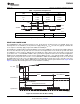
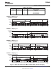
Figure 24 and Figure 25 illustrate the interface timing in slave mode and master mode, respectively.
DESCRIPTION SYMBOL MIN TYP MAX UNITS
BCK period t
(BCKP)
300 ns
BCK pulse duration, HIGH t
(BCKH)
120 ns
BCK pulse duration, LOW t
(BCKL)
120 ns
LRCK setup time to BCK rising edge t
(LRSU)
80 ns
LRCK hold time to BCK rising edge t
(LRHD)
40 ns
LRCK period t
(LRCP)
20 µ s
FSYNC setup time to BCK rising edge t
(FSSU)
40 ns
FSYNC hold time to BCK rising edge t
(FSHD)
40 ns
Delay time, BCK falling edge to DOUT valid t
(CKDO)
– 20 40 ns
Delay time, LRCK edge to DOUT valid t
(LRDO)
– 20 40 ns
Rising time of all signals t
(RISE)
20 ns
Falling time of all signals t
(FALL)
20 ns
NOTE: Timing measurement reference level is (V
IH
+ V
IL
)/2. Rising and falling time is measured from 10% to 90% of the I/O
signal swing. Load capacitance of the DOUT signal is 20 pF.
Figure 24. Audio Data Interface Timing (Slave Mode: FSYNC, LRCK, and BCK Are Inputs)
Copyright © 2000 – 2008, Texas Instruments Incorporated Submit Documentation Feedback 17
Product Folder Link(s): PCM1800