
Datasheet


APPLICATION CIRCUIT
I/V Section
Differential Section
PCM1795
SLES248 – MAY 2009 ........................................................................................................................................................................................................
www.ti.com
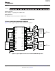
The design of the application circuit is very important in order to actually realize the high S/N ratio of which the
PCM1795 is capable, because noise and distortion that are generated in an application circuit are not negligible.
In the third-order, low-pass filter (LPF) circuit of Figure 52 , the output level of 2.1 V RMS and 123-dB
signal-to-noise ratio is achieved.
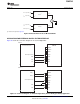
Figure 53 shows a circuit for the DSD mode, which is a fourth-order LPF in order to reduce the out-of-band
noise.
The current of the PCM1795 on each of the output pins (I
OUT
L+, I
OUT
L – , I
OUT
R+, I
OUT
R – ) is 4 mA
PP
at 0 dB
(full-scale). The voltage output level of the current-to-voltage (I/V) converter, V
I
, is given by Equation 2 :
V
I
= 4 mA
PP
× R
F
Where:
R
F
= feedback resistance of the I/V converter
An NE5534 operational amplifier is recommended for the I/V circuit to obtain the specified performance. Dynamic
performance such as the gain bandwidth, settling time, and slew rate of the operational amplifier affects the
audio dynamic performance of the I/V section.
The PCM1795 voltage outputs are followed by differential amplifier stages that sum the differential signals for
each channel, creating a single-ended I/V op-amp output. In addition, the differential amplifiers provide a
low-pass filter function.
The operational amplifier recommended for the differential circuit is the low-noise type.
36 Submit Documentation Feedback Copyright © 2009, Texas Instruments Incorporated
Product Folder Link(s): PCM1795