
Datasheet


SLES071B − MARCH 2003 − REVISED NOVEMBER 2006
www.ti.com
40
Pin Assignments When Using the DSD Format Interface
Several pins are redefined for DSD mode operation. These include:
D DATA (pin 3): DSDL as L-channel DSD data input, or as DSD data input in mono mode
D LRCK (pin 1): DSDR as R-channel DSD data input
D SCK (pin 5): DBCK as bit clock for DSD data
D BCK (pin 2): Set LOW (N/A)
Requirements for System Clock
The bit clock (DBCK) for DSD mode is required at pin 5 of the PCM1791A. The frequency of bit clock may be N times
the sampling frequency. Generally, N is 64 in DSD applications.
The interface timing between the bit clock and DSDL, DSDR is required to meet the setup and hold time specifications
shown in Figure 43.
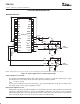
t = 1/(64 × 44.1 kHz)
D1
DSDL
DSDR
D0 D2 D3 D4
DBCK
Figure 42. Normal Data Output Form From DSD Decoder
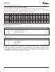
DSDL
DSDR
t
(BCH)
DBCK
t
(BCL)
t
(BCY)
1.4 V
1.4 V
t
(DS)
t
(DH)
PARAMETER MIN MAX UNITS
t
(BCY)
DBCK pulse cycle time 85
(1)
ns
t
(BCH)
DBCK high-level time 30 ns
t
(BCL)
DBCK low-level time 30 ns
t
(DS)
DSDL, DSDR setup time 10 ns
t
(DH)
DSDL, DSDR hold time 10 ns
(1)
2.8224 MHz × 4. (2.8224 MHz = 64 × 44.1 kHz. This value is specified as a
sampling rate of DSD.)
Figure 43. Timing for DSD Audio Interface