
Datasheet


www.ti.com
I
2
C Interface Timing Requirements
Switching Characteristics
PCA9545A
4-CHANNEL I
2
C AND SMBus SWITCH
WITH INTERRUPT LOGIC AND RESET FUNCTIONS
SCPS147C – OCTOBER 2005 – REVISED OCTOBER 2006
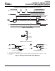
over recommended operating free-air temperature range (unless otherwise noted) (see Figure 10 )
STANDARD MODE FAST MODE
I
2
C BUS I
2
C BUS
UNIT
MIN MAX MIN MAX
f
scl
I
2
C clock frequency 0 100 0 400 kHz
t
sch
I
2
C clock high time 4 0.6 µ s
t
scl
I
2
C clock low time 4.7 1.3 µ s
t
sp
I
2
C spike time 50 50 ns
t
sds
I
2
C serial-data setup time 250 100 ns
t
sdh
I
2
C serial-data hold time 0
(1)
0
(1)
µ s
t
icr
I
2
C input rise time 1000 20 + 0.1C
b
(2)
300 ns
t
icf
I
2
C input fall time 300 20 + 0.1C
b
(2)
300 ns
t
ocf
I
2
C output fall time 10-pF to 400-pF bus 300 20 + 0.1C
b
(2)
300 ns
t
buf
I
2
C bus free time between stop and start 4.7 1.3 µ s
t
sts
I
2
C start or repeated start condition setup 4.7 0.6 µ s
t
sth
I
2
C start or repeated start condition hold 4 0.6 µ s
t
sps
I
2
C stop condition setup 4 0.6 µ s
SCL low to SDA output low
t
vdL(Data)
Valid-data time (high to low)
(3)
1 1 µ s
valid
SCL low to SDA output high
t
vdH(Data)
Valid-data time (low to high)
(3)
0.6 0.6 µ s
valid
ACK signal from SCL low
t
vd(ack)
Valid-data time of ACK condition 1 1 µ s
to SDA output low
C
b
I
2
C bus capacitive load 400 400 pF
(1) A device internally must provide a hold time of at least 300 ns for the SDA signal (referred to as the V
IH
min of the SCL signal), in order
to bridge the undefined region of the falling edge of SCL.
(2) C
b
= total bus capacitance of one bus line in pF
(3) Data taken using a 1-k Ω pullup resistor and 50-pF load (see Figure 10 )
over recommended operating free-air temperature range, C
L
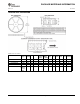
≤ 100 pF (unless otherwise noted) (see Figure 12 )
FROM TO
PARAMETER MIN MAX UNIT
(INPUT) (OUTPUT)
R
ON
= 20 Ω , C
L
= 15 pF 0.3
t
pd
(1)
Propagation delay time SDA or SCL SDn or SCn ns
R
ON
= 20 Ω , C
L
= 50 pF 1
t
iv
Interrupt valid time
(2)
INTn INT 4 µ s
t
ir
Interrupt reset delay time
(2)
INTn INT 2 µ s
(1) The propagation delay is the calculated RC time constant of the typical ON-state resistance of the switch and the specified load
capacitance, when driven by an ideal voltage source (zero output impedance).
(2) Data taken using a 4.7-k Ω pullup resistor and 100-pF load (see Figure 12 )
12
Submit Documentation Feedback