
Datasheet


PCA9539
www.ti.com
SCPS130F –AUGUST 2005–REVISED JANUARY 2011
Register Descriptions
The Input Port registers (registers 0 and 1) reflect the incoming logic levels of the pins, regardless of whether the
pin is defined as an input or an output by the Configuration register. It only acts on read operation. Writes to
these registers have no effect. The default value, X, is determined by the externally applied logic level.
Before a read operation, a write transmission is sent with the command byte to indicate to the I
2
C device that the
Input Port register will be accessed next.
Table 4. Registers 0 and 1 (Input Port Registers)
Bit I0.7 I0.6 I0.5 I0.4 I0.3 I0.2 I0.1 I0.0
Default X X X X X X X X
Bit I1.7 I1.6 I1.5 I1.4 I1.3 I1.2 I1.1 I1.0
Default X X X X X X X X
The Output Port registers (registers 2 and 3) show the outgoing logic levels of the pins defined as outputs by the
Configuration register. Bit values in this register have no effect on pins defined as inputs. In turn, reads from this
register reflect the value that is in the flip-flop controlling the output selection, not the actual pin value.
Table 5. Registers 2 and 3 (Output Port Registers)
Bit O0.7 O0.6 O0.5 O0.4 O0.3 O0.2 O0.1 O0.0
Default 1 1 1 1 1 1 1 1
Bit O1.7 O1.6 O1.5 O1.4 O1.3 O1.2 O1.1 O1.0
Default 1 1 1 1 1 1 1 1
The Polarity Inversion registers (registers 4 and 5) allow Polarity Inversion of pins defined as inputs by the
Configuration register. If a bit in this register is set (written with 1), the corresponding port pin's polarity is
inverted. If a bit in this register is cleared (written with a 0), the corresponding port pin's original polarity is
retained.
Table 6. Registers 4 and 5 (Polarity Inversion Registers)
Bit N0.7 N0.6 N0.5 N0.4 N0.3 N0.2 N0.1 N0.0
Default 0 0 0 0 0 0 0 0
Bit N1.7 N1.6 N1.5 N1.4 N1.3 N1.2 N1.1 N1.0
Default 0 0 0 0 0 0 0 0
The Configuration registers (registers 6 and 7) configure the directions of the I/O pins. If a bit in this register is
set to 1, the corresponding port pin is enabled as an input with a high-impedance output driver. If a bit in this
register is cleared to 0, the corresponding port pin is enabled as an output.
Table 7. Registers 6 and 7 (Configuration Registers)
Bit C0.7 C0.6 C0.5 C0.4 C0.3 C0.2 C0.1 C0.0
Default 1 1 1 1 1 1 1 1
Bit C1.7 C1.6 C1.5 C1.4 C1.3 C1.2 C1.1 C1.0
Default 1 1 1 1 1 1 1 1
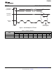
Power-On Reset
When power (from 0 V) is applied to V
CC
, an internal power-on reset holds the PCA9539 in a reset condition until
V
CC
has reached V
POR
. At that point, the reset condition is released and the PCA9539 registers and I
2
C/SMBus
state machine initialize to their default states. After that, V
CC
must be lowered to below 0.2 V and then back up to
the operating voltage for a power-reset cycle.
Copyright © 2005–2011, Texas Instruments Incorporated Submit Documentation Feedback 9
Product Folder Link(s): PCA9539