
Datasheet


V
CC
Ramp-Up
Time to Re-Ramp
Time
Ramp-Down
V
IN
drops below POR levels
V
CC_RT
V
CC_FT
V
CC_TRR_VPOR50
V
CC
Time
V
CC_GH
V
CC_GW
PCA9534
SCPS124G –SEPTEMBER 2006–REVISED JUNE 2010
www.ti.com
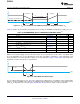
Figure 18. V
CC
is Lowered Below the POR Threshold, Then Ramped Back Up to V
CC
Table 10 specifies the performance of the power-on reset feature for PCA9534 for both types of power-on reset.
Table 10. RECOMMENDED SUPPLY SEQUENCING AND RAMP RATES
(1)
PARAMETER MIN TYP MAX UNIT
V
CC_FT
Fall rate See Figure 17 1 100 ms
V
CC_RT
Rise rate See Figure 17 0.01 100 ms
V
CC_TRR_GND
Time to re-ramp (when V
CC
drops to GND) See Figure 17 0.001 ms
V
CC_TRR_POR50
Time to re-ramp (when V
CC
drops to V
POR_MIN
– 50 mV) See Figure 18 0.001 ms
Level that V
CCP
can glitch down to, but not cause a functional
V
CC_GH
See Figure 19 1.2 V
disruption when V
CCX_GW
= 1 ms
Glitch width that will not cause a functional disruption when
V
CC_GW
See Figure 19 ms
V
CCX_GH
= 0.5 × V
CCx
V
PORF
Voltage trip point of POR on falling V
CC
0.767 1.144 V
V
PORR
Voltage trip point of POR on fising V
CC
1.033 1.428 V
(1) T
A
= –40°C to 85°C (unless otherwise noted)
Glitches in the power supply can also affect the power-on reset performance of this device. The glitch width
(V
CC_GW
) and height (V
CC_GH
) are dependent on each other. The bypass capacitance, source impedance, and
device impedance are factors that affect power-on reset performance. Figure 19 and Table 10 provide more
information on how to measure these specifications.
Figure 19. Glitch Width and Glitch Height
V
POR
is critical to the power-on reset. V
POR
is the voltage level at which the reset condition is released and all the
registers and the I
2
C/SMBus state machine are initialized to their default states. The value of V
POR
differs based
on the V
CC
being lowered to or from 0. Figure 20 and Table 10 provide more details on this specification.
24 Submit Documentation Feedback Copyright © 2006–2010, Texas Instruments Incorporated
Product Folder Link(s): PCA9534