
Datasheet


www.ti.com
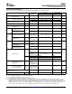
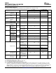
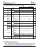
Electrical Characteristics
P82B96
DUAL BIDIRECTIONAL BUS BUFFER
SCPS144B – MAY 2006 – REVISED JULY 2007
V
CC
= 3 V to 3.6 V, voltages are specified with respect to GND (unless otherwise noted)
T
A
= 25 ° C T
A
= –40 ° C to 85 ° C
PARAMETER TEST CONDITIONS UNIT
MIN TYP
(1)
MAX MIN MAX
Temperature
Δ V/ Δ T
IN
coefficient of Sx, Sy –2 mV/ ° C
input thresholds
I
Sx
, I
Sy
= 3 mA 0.8 0.88 1
Low-level output
V
OL
Sx, Sy
(2)
V
voltage
I
Sx
, I
Sy
= 0.2 mA 0.67 0.73 0.79
(2)
Temperature
coefficient of
Δ V/ Δ T
OUT
Sx, Sy I
Sx
, I
Sy
= 0.2 mA –1.8 mV/ ° C
output low
levels
(3)
I
CC
Quiescent supply current Sx = Sy = V
CC
0.9 1.8 2 mA
Additional supply
Δ I
CC
current per pin Tx, Ty 1.7 2.75 3 mA
low
Dynamic output
V
Sx
, V
Sy
> 2 V,
sink capability 7 18 5.7 mA
V
Rx
, V
Ry
= low
on I
2
C bus
I
IOS
Sx, Sy
Leakage current V
Sx
, V
Sy
= 5 V,
0.1 1 1 μ A
on I
2
C bus V
Rx
, V
Ry
= high
Dynamic output V
Tx
, V
Ty
> 1 V,
sink capability V
Sx
, V
Sy
= low on I
2
C 60 100 60 mA
on buffered bus bus = 0.4 V
I
IOT
Tx, Ty
Leakage current V
Tx
, V
Ty
= V
CC
=
0.1 1 1 μ A
on buffered bus 3.3 V, V
Sx
, V
Sy
= high
Input current Bus low, V
Rx
,
Sx, Sy –1 1
from I
2
C bus V
Ry
= high
Input current Bus low, V
Rx
,
–1 1
I
I
from buffered bus V
Ry
= 0.4 V μ A
Rx, Ry
Leakage current
on buffered bus V
Rx
, V
Ry
= V
CC
1 1.5
input
Input logic-level high
threshold
(4)
0.65 0.7
(2)
on normal I
2
C bus
Sx, Sy
Input logic-level low
threshold
(4)
0.6 0.65
(2)
V
IT
Input threshold V
on normal I
2
C bus
Input logic level high 0.58 V
CC
0.58 V
CC
Rx, Ry Input threshold 0.5 V
CC
Input logic level low 0.42 V
CC
0.42 V
CC
(V
Sx
output low
Input/output logic at 3 mA) –
V
IOdiff
Sx, Sy 100 150 100 mV
level difference
(5)
(V
Sx
input high max)
for I
2
C applications
Sx, Sy are low, V
CC
V
CC
voltage at
Sx, Sy ramping, voltage on
V
IOrel
which all buses 1 1 V
Tx, Ty Tx, Ty lowered until
are released
released
(1) Typical value is at V
CC
= 3.3 V, T
A
= 25 ° C
(2) See the Typical Characteristics section of this data sheet.
(3) The output logic low depends on the sink current.
(4) The input logic threshold is independent of the supply voltage.
(5) The minimum value requirement for pullup current, 200 μ A, ensures that the minimum value for V
SX
output low always exceeds the
minimum V
Sx
input high level to eliminate any possibility of latching. The specified difference is specified by design within any device.
While the tolerances on absolute levels allow a small probability that the low from one Sx output is recognized by an Sx input of another
P82B96, this has no consequences for normal applications. In any design, the Sx pins of different devices never should be linked,
because the resulting system would be very susceptible to induced noise and would not support all I
2
C operating modes.
6
Submit Documentation Feedback