
Datasheet


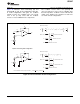


V
OUT
=
-V CODE
REF
´
65536
DAC8811
C
2
C
1
V
DD
R
FB
I
OUT
GND
V
REF
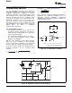
+10V
V
OUT
-10V V +10V
OUT
£ £
10kW
10kW
5kW
OPA827
OPA827
OPA827
SBOS376H –NOVEMBER 2006–REVISED MAY 2012
www.ti.com
OPA827 USED AS AN I/V CONVERTER NOTE: CODE is the digital input into the DAC.
The OPA827 series of operation amplifiers have low The DAC output impedance as seen looking into the
current noise and offset voltage that make these I
OUT
terminal changes versus code. The low offset
devices a great choice for an I/V converter. The voltage of the OPA827 minimizes the error
DAC8811 is a single channel, current output, 16-bit propagated from the DAC.
digital-to-analog converter (DAC). The I
OUT
terminal
For a current-to-voltage design (see Figure 49), the
of the DAC is held at a virtual GND potential by the
DAC8811 I
OUT
pin and the inverting node of the
use of the OPA827 as an external I/V converter op
OPA827 should be as short as possible and adhere
amp. The R-2R ladder is connected to an external
to good PCB layout design. For each code change on
reference input (V
REF
) that determines the DAC full-
the output of the DAC, there is a step function. If the
scale current. The external reference voltage can
parasitic capacitance is excessive at the inverting
vary in a range of –15V to +15V, thus providing
node, then gain peaking is possible. For circuit
bipolar I
OUT
current operation. By using the OPA827
stability, two compensation capacitors, C
1
and C
2
(4pF
as an external I/V converter in conjunction with the
to 20pF typical) can be added to the design.
internal DAC8811 R
FB
resistor, output voltage ranges
of –V
REF
to +V
REF
can be generated.
Some applications require full four-quadrant
multiplying capabilities or a bipolar output swing. As
When using an external I/V converter and the
shown in Figure 49, the OPA827 is added as a
DAC8811 R
FB
resistor, the DAC output voltage is
summing amp and has a gain of 2x that widens the
given by Equation 3.
output span to 20V. A four-quadrant multiplying circuit
is implemented by using a 10V offset of the reference
voltage to bias the OPA827.
(3)
Figure 49. I/V Converter
18 Copyright © 2006–2012, Texas Instruments Incorporated