
Datasheet


"#$
SBOS303C − JUNE 2004 − REVISED AUGUST 2008
www.ti.com
16
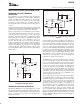
SINGLE OP AMP DIFFERENTIAL AMPLIFIER
The voltage-feedback architecture of the OPA820, with its
high common-mode rejection ratio (CMRR), will provide
exceptional performance in differential amplifier configura-
tions. Figure 6 shows a typical configuration. The starting
point for this design is the selection of the R
F
value in the range
of 200Ω to 2kΩ. Lower values reduce the required R
G
,
increasing the load on the V
2
source and on the OPA820
output. Higher values increase output noise as well as the
effects of parasitic board and device capacitances. Following
the selection of R
F
, R
G
must be set to achieve the desired
inverting gain for V
2
. Remember that the bandwidth will be set
approximately by the gain bandwidth product (GBP) divided
by the noise gain (1 + R
F
/R
G
). For accurate differential
operation (that is, good CMRR), the ratio R
2
/R
1
must be set
equal to R
F
/R
G
.
OPA820
+5V
−
5V
R
2
50Ω
Power−supply decoupling not shown.
V
2
R
1
V
1
R
F
R
G
V
O
=(V
1
− V
2
)
R
F
R
G
when =
R
2
R
1
R
F
R
G
Figure 6. High-Speed, Single Differential
Amplifier
Usually, it is best to set the absolute values of R
2
and R
1
equal
to R
F
and R
G
, respectively; this equalizes the divider
resistances and cancels the effect of input bias currents.
However, it is sometimes useful to scale the values of R
2
and
R
1
in order to adjust the loading on the driving source, V
1
. In
most cases, the achievable low-frequency CMRR will be
limited by the accuracy of the resistor values. The 85dB
CMRR of the OPA820 itself will not determine the overall circuit
CMRR unless the resistor ratios are matched to better than
0.003%. If it is necessary to trim the CMRR, then R
2
is the
suggested adjustment point.
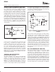
THREE OP AMP DIFFERENCING
(Instrumentation Topology)
The primary drawback of the single op amp differential
amplifier is its relatively low input impedances. Where high
impedance is required at the differential input, a standard
instrumentation amplifier (INA) topology may be built using the
OPA820 as the differencing stage. Figure 7 shows an
example of this, in which the two input amplifiers are packaged
together as a dual voltage-feedback op amp, the OPA2822.
This approach saves board space, cost, and power compared
to using two additional OPA820 devices, and still achieves
very good noise and distortion performance as a result of the
moderate loading on the input amplifiers.
OPA820
Power−supply decoupling not shown.
V
O
V
1
R
G
500
Ω
V
2
OPA2822
+5V
+5V
−
5V
−
5V
OPA2822
500
Ω
500
Ω
R
F1
500
Ω
500
Ω
500
Ω
R
F1
500
Ω
Figure 7. Wideband 3-Op Amp Differencing
Amplifier
In this circuit, the common-mode gain to the output is always
1, because of the four matched 500Ω resistors, whereas the
differential gain is set by (1 + 2R
F1
/R
G
), which is equal to 2
using the values in Figure 7. The differential to single-ended
conversion is still performed by the OPA820 output stage. The
high-impedance inputs allow the V
1
and V
2
sources to be
terminated or impedance-matched as required. If the V
1
and
V
2
inputs are already truly differential, such as the output from
a signal transformer, then a single matching termination
resistor may be used between them. Remember, however,
that a defined DC signal path must always exist for the V
1
and
V
2
inputs; for the transformer case, a center-tapped secon-
dary connected to ground would provide an optimum DC
operating point.
DAC TRANSIMPEDANCE AMPLIFIER
High-frequency Digital-to-Analog Converters (DACs) require
a low-distortion output amplifier to retain their SFDR
performance into real-world loads. See Figure 8 for a
single-ended output drive implementation. In this circuit, only
one side of the complementary output drive signal is used. The
diagram shows the signal output current connected into the
virtual ground-summing junction of the OPA820, which is set
up as a transimpedance stage or I-V converter. The unused
current output of the DAC is connected to ground. If the DAC
requires its outputs to be terminated to a compliance voltage
other than ground for operation, then the appropriate voltage
level may be applied to the noninverting input of the OPA820.