
Datasheet


"#$% &"#$
"#'% &"#'
SBOS282B − DECEMBER 2003 − REVISED FEBRUARY 2005
www.ti.com
9
Low-gain (< 20) operation demands that the auto-zero
circuitry correct for common-mode rejection errors of the
main amplifier. Because these errors can be larger than
0.1% of a full-scale input step change, one calibration
cycle (100µs) can be required to achieve full accuracy.
The term clock feedthrough describes the presence of the
clock frequency in the output spectrum. In auto-zeroed op
amps, clock feedthrough may result from the settling of the
internal sampling capacitor, or from the small amount of
charge injection that occurs during the sample-and-hold of
the op amp offset voltage. Feedthrough can be minimized
by keeping the source impedance relatively low (< 1kΩ)
and matching the source impedance on both input
terminals. If the source resistance is high (> 1kΩ)
feedthrough can generally be reduced with a capacitor of
1nF or greater in parallel with the source or feedback
resistors. See the circuit application examples.
LAYOUT GUIDELINES
Attention to good layout practices is always recom-
mended. Keep traces short. When possible, use a PCB
ground plane with surface-mount components placed as
close to the device pins as possible. Place a 0.1µF
capacitor closely across the supply pins. These guidelines
should be applied throughout the analog circuit to improve
performance and provide benefits such as reducing the
electromagnetic-interference (EMI) susceptibility.
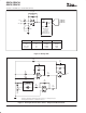
R
1
V
EX
V
OUT
V
REF
R
1
OPA734
R
R
RR
+10V
1nF
1nF
Figure 2. Single Op Amp Bridge Amplifier Circuit
1/2
OPA2735
R
3
10k
Ω
R
3
10k
Ω
R
1
1k
Ω
1/2
OPA2735
R
2
1k
Ω
C
4
1nF
C
4
1nF
R
G
10V
C
1
(1)
1nF
C
2
(1)
10nF
C
3
(1)
1nF
V
REF
= 15V
2
4
6
REF102
NOTE: (1) Place close to input pins.
R
R
RR
G=1+2
R
3
R
G
Figure 3. Differential Output Bridge Amplifier