
Datasheet


8
OPA353, 2353, 4353
®
APPLICATIONS INFORMATION
OPA353 series op amps are fabricated on a state-of-the-art
0.6 micron CMOS process. They are unity-gain stable and
suitable for a wide range of general purpose applications.
Rail-to-rail input/output make them ideal for driving sam-
pling A/D converters. They are well suited for controlling
the output power in cell phones. These applications often
require high speed and low noise. In addition, the OPA353
series offers a low cost solution for general purpose and
consumer video applications (75Ω drive capability).
Excellent ac performance makes the OPA353 series well
suited for audio applications. Their bandwidth, slew rate,
low noise (5nV/√Hz), low THD (0.0006%), and small pack-
age options are ideal for these applications. The class AB
output stage is capable of driving 600Ω loads connected to
any point between V+ and ground.
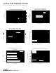
Rail-to-rail input and output swing significantly increases
dynamic range, especially in low voltage supply applica-
tions. Figure 1 shows the input and output waveforms for
the OPA353 in unity-gain configuration. Operation is
from a single +5V supply with a 1kΩ load connected to
V
S
/2. The input is a 5Vp-p sinusoid. Output voltage is
approximately 4.95Vp-p.
Power supply pins should be bypassed with 0.01µF ceramic
capacitors.
OPERATING VOLTAGE
OPA353 series op amps are fully specified from +2.7V to
+5.5V. However, supply voltage may range from +2.5V to
+5.5V. Parameters are guaranteed over the specified supply
range—a unique feature of the OPA353 series. In addition,
many specifications apply from –40°C to +85°C. Most
behavior remains virtually unchanged throughout the full
operating voltage range. Parameters which vary signifi-
cantly with operating voltages or temperature are shown in
the typical performance curves.
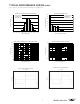
RAIL-TO-RAIL INPUT
The guaranteed input common-mode voltage range of the
OPA353 series extends 100mV beyond the supply rails. This
is achieved with a complementary input stage—an
N-channel input differential pair in parallel with a P-channel
differential pair (see Figure 2). The N-channel pair is active
for input voltages close to the positive rail, typically
(V+) – 1.8V to 100mV above the positive supply, while the
P-channel pair is on for inputs from 100mV below the
negative supply to approximately (V+) – 1.8V. There is a
small transition region, typically (V+) – 2V to (V+) – 1.6V, in
which both pairs are on. This 400mV transition region can
vary ±400mV with process variation. Thus, the transition
region (both input stages on) can range from (V+) – 2.4V to
(V+) – 2.0V on the low end, up to (V+) – 1.6V to (V+) – 1.2V
on the high end.
FIGURE 2. Simplified Schematic.
V
BIAS1
V
BIAS2
V
IN
+
V
IN
–
Class AB
Control
Circuitry
V
O
V–
(Ground)
V+
Reference
Current
0
5V
V
S
= +5, G = +1, R
L
= 1kΩ
V
IN
1.25V/div
FIGURE 1. Rail-to-Rail Input and Output.
5V
0
V
OUT