
Datasheet


OPA322, OPA322S
OPA2322, OPA2322S
OPA4322, OPA4322S
SBOS538E –JANUARY 2011–REVISED JUNE 2012
www.ti.com
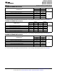
ELECTRICAL CHARACTERISTICS: V
S
= +1.8 V to +5.5 V, or ±0.9 V to ±2.75 V (continued)
Boldface limits apply over the specified temperature range, T
A
= –40°C to +125°C.
At T
A
= +25°C, R
L
= 10 kΩ connected to V
S
/2, V
CM
= V
S
/2, V
OUT
= V
S
/2, and SHDN_x = V
S
+, unless otherwise noted.
OPA322, OPA322S, OPA2322,
OPA2322S, OPA4322, OPA4322S
PARAMETER TEST CONDITIONS MIN TYP MAX UNIT
OUTPUT
Voltage output swing from
V
O
R
L
= 10 kΩ 10 20 mV
both rails
Over temperature R
L
= 10 kΩ 30 mV
Short-circuit current I
SC
V
S
= 5.5 V ±65 mA
Capacitive load drive C
L
See Typical Characteristics
Open-loop output resistance R
O
I
O
= 0 mA, f = 1 MHz 90 Ω
POWER SUPPLY
Specified voltage range V
S
1.8 5.5 V
Quiescent current per amplifier I
Q
I
O
= 0 mA, V
S
= +5.5 V
OPA322, OPA322S I
O
= 0 mA, V
S
= +5.5 V 1.6 1.9 mA
Over temperature I
O
= 0 mA, V
S
= +5.5 V 2 mA
OPA2322, OPA2322S I
O
= 0 mA, V
S
= +5.5 V 1.5 1.75 mA
Over temperature I
O
= 0 mA, V
S
= +5.5 V 1.85 mA
OPA4322, OPA4322S I
O
= 0 mA, V
S
= +5.5 V 1.4 1.65 mA
Over temperature I
O
= 0 mA, V
S
= +5.5 V 1.75 mA
Power-on time V
S+
= 0 V to 5 V, to 90% I
Q
level 28 μs
SHUTDOWN
(2)
V
S
= 1.8 V to 5.5 V
Quiescent current, per amplifier I
QSD
All amplifiers disabled, SHDN = V
S–
0.1 0.5 µA
High voltage (enabled) V
IH
Amplifier enabled (V+) - 0.1 V
Low voltage (disabled) V
IL
Amplifier disabled (V-) + 0.1 V
Amplifier enable time (full
t
ON
Full shutdown; G = 1, V
OUT
= 0.9 × V
S
/2
(4)
10 µs
shutdown)
(3)
Amplifier enable time (partial
t
ON
Partial shutdown; G = 1, V
OUT
= 0.9 × V
S
/2
(4)
6 µs
shutdown)
(3)
Amplifier disable time
(3)
t
OFF
G = 1, V
OUT
= 0.1 × V
S
/2 3 µs
V
IH
= 5.0 V 0.13 µA
SHDN pin input bias current (per pin)
V
IL
= 0 V 0.04 µA
TEMPERATURE
Specified range –40 +125 °C
Operating range –40 +150 °C
(2) Ensured by design and characterization; not production tested.
(3) Disable time (t
OFF
) and enable time (t
ON
) are defined as the time interval between the 50% point of the signal applied to the SHDN pin
and the point at which the output voltage reaches the 10% (disable) or 90% (enable) level.
(4) Full shutdown refers to the dual OPA2322S having both channels A and B disabled (SHDN_A = SHDN_B = V
S–
) and the quad
OPA4322S having all channels A to D disabled (SHDN_A/B = SHDN_C/D = V
S–
). For partial shutdown, only one SHDN pin is exercised;
in this mode, the internal biasing and oscillator remain operational and the enable time is shorter.
4 Submit Documentation Feedback Copyright © 2011–2012, Texas Instruments Incorporated
Product Folder Link(s): OPA322 OPA322S OPA2322 OPA2322S OPA4322 OPA4322S