
Datasheet


APPLICATION INFORMATION
WIDEBAND VOLTAGE-FEEDBACK
1/3
OPA3832
V =+3.3V
S
V
OUT
66.5W
V
IN
1.13kW
255W
R
L
150W
0.75V
6.8 Fm
+
0.1 Fm
0.1 Fm
400W400W
+0.75V
+0.75
1/3
OPA3832
V =+5V
S
V
OUT
66.7W
V
IN
505W
+2V
332W
R
L
150W
+2V
6.8 Fm
+
0.1 Fm
0.1 Fm
400W400W
2V
OPA3832
SBOS370A – DECEMBER 2006 – REVISED AUGUST 2008 ............................................................................................................................................
www.ti.com
effective load on the output at high frequencies is
150 Ω || 800 Ω . The 255 Ω and 1.13k Ω resistors at the
noninverting input provide the common-mode bias
OPERATION
voltage. This parallel combination equals the dc
The OPA3832 is a unity-gain stable, very high-speed
resistance at the inverting input R
F
), reducing the dc
voltage-feedback op amp designed for single-supply
output offset arising from input bias current.
operation (+3V to +11V). The input stage supports
input voltages below ground and to within 1.7V of the
positive supply. The complementary common-emitter
output stage provides an output swing to within 25mV
of ground and the positive supply. The OPA3832 is
compensated to provide stable operation with a wide
range of resistive loads.
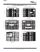
Figure 46 shows the ac-coupled, gain of +2V/V
configuration used for the +5V Specifications and
Typical Characteristic Curves. For test purposes, the
input impedance is set to 50 Ω with the 66.7 Ω resistor
to ground in parallel with the 200 Ω bias network.
Voltage swings reported in the Electrical
Characteristics are taken directly at the input and
output pins. For the circuit of Figure 46 , the total
effective load on the output at high frequencies is
Figure 47. AC-Coupled, G = +2, +3.3V
150 Ω || 800 Ω . The 332 Ω and 505 Ω resistors at the Single-Supply Specification and Test Circuit
noninverting input provide the common-mode bias
voltage. This parallel combination equals the dc
Figure 48 shows the dc-coupled, gain of +2, dual
resistance at the inverting input R
F
), reducing the dc
power-supply circuit configuration used as the basis
output offset resulting from input bias current.
of the ± 5V Electrical Characteristics and Typical
Characteristics. For test purposes, the input
impedance is set to 50 Ω with a resistor to ground and
the output impedance is set to 150 Ω with a series
output resistor. Voltage swings reported in the
specifications are taken directly at the input and
output pins. For the circuit of Figure 48 , the total
effective load will be 150 Ω || 800 Ω . Two optional
components are included in Figure 48 . An additional
resistor (175 Ω ) is included in series with the
noninverting input. Combined with the 25 Ω dc source
resistance looking back towards the signal generator,
this configuration gives an input bias current
cancelling resistance that matches the 200 Ω source
resistance seen at the inverting input (see the DC
Accuracy and Offset Control section). In addition to
the usual power-supply decoupling capacitors to
Figure 46. AC-Coupled, G = +2, +5V Single-Supply
ground, a 0.01 µ F capacitor is included between the
Specification and Test Circuit
two power-supply pins. In practical printed circuit
board (PCB) board layouts, this optional capacitor will
Figure 47 shows the ac-coupled, gain of +2V/V typically improve the 2nd-harmonic distortion
configuration used for the +3.3V Specifications and performance by 3dB to 6dB.
Typical Characteristic Curves. For test purposes, the
input impedance is set to 66.5 Ω with a resistor to
ground. Voltage swings reported in the Electrical
Characteristics are taken directly at the input and
output pins. For the circuit of Figure 47 , the total
18 Submit Documentation Feedback Copyright © 2006 – 2008, Texas Instruments Incorporated
Product Folder Link(s): OPA3832