
Datasheet


5kW
OPA348
10mA max
+5V
V
IN
V
OUT
I
OVERLOAD
10 toW
20W
OPA348
V+
V
IN
V
OUT
R
S
R
L
C
L
5V
1V/div
0V
G = +1V/V, V = +5V
S
10 s/divm
V
IN
V
OUT
OPA348
OPA2348
OPA4348
www.ti.com
SBOS213G –NOVEMBER 2001–REVISED MARCH 2013
RAIL-TO-RAIL INPUT RAIL-TO-RAIL OUTPUT
The input common-mode range extends from (V–) – A class AB output stage with common-source
0.2V to (V+) + 0.2V. For normal operation, inputs transistors is used to achieve rail-to-rail output. This
should be limited to this range. The absolute output stage is capable of driving 5kΩ loads
maximum input voltage is 500mV beyond the connected to any potential between V+ and ground.
supplies. Inputs greater than the input common-mode For light resistive loads (> 100kΩ), the output voltage
range but less than the maximum input voltage, while can typically swing to within 18mV from supply rail.
not valid, will not cause any damage to the op amp. With moderate resistive loads (10kΩ to 50kΩ), the
Unlike some other op amps, if input current is limited output voltage can typically swing to within 100mV of
the inputs may go beyond the power supplies without the supply rails while maintaining high open-loop gain
phase inversion, as shown in Figure 21. (see the typical characteristic Output Voltage Swing
vs Output Current, Figure 6).
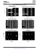
CAPACITIVE LOAD AND STABILITY
The OPA348 in a unity-gain configuration can directly
drive up to 250pF pure capacitive load. Increasing the
gain enhances the amplifier’s ability to drive greater
capacitive loads (see the typical characteristic Small-
Signal Overshoot vs Capacitive Load, Figure 13). In
unity-gain configurations, capacitive load drive can be
improved by inserting a small (10Ω to 20Ω) resistor,
R
S
, in series with the output, as shown in Figure 23.
This significantly reduces ringing while maintaining
DC performance for purely capacitive loads.
However, if there is a resistive load in parallel with
the capacitive load, a voltage divider is created,
Figure 21. OPA348—No Phase Inversion with
introducing a Direct Current (DC) error at the output
Inputs Greater than the Power-Supply Voltage
and slightly reducing the output swing. The error
introduced is proportional to the ratio R
S
/R
L
, and is
generally negligible.
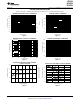
Normally, input currents are 0.5pA. However, large
inputs (greater than 500mV beyond the supply rails)
can cause excessive current to flow in or out of the
input pins. Therefore, as well as keeping the input
voltage below the maximum rating, it is also important
to limit the input current to less than 10mA. This is
easily accomplished with an input voltage resistor, as
shown in Figure 22.
Figure 23. Series Resistor in Unity-Gain Buffer
Configuration Improves Capacitive Load Drive
Figure 22. Input Current Protection for Voltages
Exceeding the Supply Voltage
Copyright © 2001–2013, Texas Instruments Incorporated Submit Documentation Feedback 9
Product Folder Links: OPA348 OPA2348 OPA4348