
Datasheet


OPA330
3V
1MW 60kW
100kW
1MW
NTC
Thermistor
IN-
IN+
OUT
V
S
-
V +
S
C3
B2
A3
C1
A1
YFFPACKAGE
WCSP-5
(TOPVIEW)
(Bumpsidedown;
nottoscale)
ActualSize:
ExactSize(max):
0,862mmx1,156mm
YFFPACKAGE
WCSP-5EnlargedImage
(TopView)
(Bumpsidedown)
PackageMarkingCode:
YMD=year/month/day
TBD=indicatesOPA330AIYFF
S=forengineeringpurposesonly
YMDTBDS
OPA330
OPA2330
OPA4330
SBOS432E –AUGUST 2008– REVISED FEBRUARY 2011
www.ti.com
R
N
are operational resistors used to isolate the Following these guidelines reduces the likelihood of
ADS1100 from the noise of the digital I
2
C bus. junctions being at different temperatures, which can
Because the ADS1100 is a 16-bit converter, a precise cause thermoelectric voltages of 0.1μV/°C or higher,
reference is essential for maximum accuracy. If depending on materials used.
absolute accuracy is not required, and the 5V power
supply is sufficiently stable, the REF3130 may be
OPA330 WCSP
omitted.
The OPA330 YFF package is a lead- (Pb-) free,
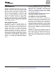
Figure 23 shows the OPA330 in a typical thermistor
die-level, wafer chip-scale package (WCSP). Unlike
circuit.
devices that are in plastic packages, these devices
have no molding compound, lead frame, wire bonds,
or leads. Using standard surface-mount assembly
procedures, the WCSP can be mounted to a printed
circuit board (PCB) without additional underfill.
Figure 24 and Figure 25 detail the pinout and
package marking, respectively. See the NanoStar™
and NanoFree™ 300μm Solder Bump WCSP
Application Note (SBVA017) for more detailed
information on package characteristics and PCB
design.
Figure 23. Thermistor Measurement
GENERAL LAYOUT GUIDELINES
Attention to good layout practice is always
recommended. Keep traces short and, when
possible, use a printed circuit board (PCB) ground
plane with surface-mount components placed as
close to the device pins as possible. Place a 0.1μF
capacitor closely across the supply pins. These
guidelines should be applied throughout the analog
circuit to improve performance and provide benefits
such as reducing the electromagnetic interference
Figure 24. WCSP Pin Description
(EMI) susceptibility.
For lowest offset voltage and precision performance,
circuit layout and mechanical conditions should be
optimized. Avoid temperature gradients that create
thermoelectric (Seebeck) effects in the thermocouple
junctions formed from connecting dissimilar
conductors. These thermally-generated potentials can
be made to cancel by assuring they are equal on
both input terminals. Other layout and design
considerations include:
• Use low thermoelectric-coefficient conditions
(avoid dissimilar metals).
• Thermally isolate components from power
Figure 25. YFF Package Marking
supplies or other heat sources.
• Shield op amp and input circuitry from air
currents, such as cooling fans.
12 Submit Documentation Feedback © 2008–2011, Texas Instruments Incorporated
Product Folder Link(s): OPA330 OPA2330 OPA4330