
Datasheet


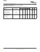


ELECTRICAL CHARACTERISTICS: V
S
= +3.3V
OPA2832
www.ti.com
............................................................................................................................................. SBOS327C – FEBRUARY 2005 – REVISED AUGUST 2008
Boldface limits are tested at +25 ° C.
At T
A
= +25 ° C, G = +2V/V, and R
L
= 150 Ω to V
CM
= 0.75V, unless otherwise noted (see Figure 62 ).
OPA2832ID, IDGK
0 ° C to MIN/ TEST
PARAMETER CONDITIONS +25 ° C +25 ° C
(1)
+70 ° C
(2)
UNITS MAX LEVEL
(3)
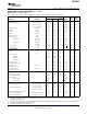
AC PERFORMANCE (see Figure 62 )
Small-Signal Bandwidth G = +1, V
O
≤ 0.5V
PP
180 MHz typ C
G = +2, V
O
≤ 0.5V
PP
85 59 57 MHz min B
G = – 1, V
O
≤ 0.5V
PP
100 63 61 MHz min B
Peaking at a Gain of +1 V
O
≤ 0.5V
PP
8 dB typ C
Slew Rate 1V Step 130 110 100 V/ µ s min B
Rise Time 0.5V Step 4.6 5.6 5.7 ns max B
Fall Time 0.5V Step 4.6 5.6 5.7 ns max B
Settling Time to 0.1% 1V Step 48 70 80 ns max B
Harmonic Distortion 5MHz
2nd-Harmonic R
L
= 150 Ω – 71 – 64 – 61 dBc max B
R
L
= 500 Ω – 74 – 70 – 64 dBc max B
3rd-Harmonic R
L
= 150 Ω – 66 – 60 – 55 dBc max B
R
L
= 500 Ω – 69 – 66 – 62 dBc max B
Input Voltage Noise f > 1MHz 9.4 nV/ √ Hz typ C
Input Current Noise f > 1MHz 2.4 pA/ √ Hz typ C
DC PERFORMANCE
(4)
Gain Error G = +2 ± 0.3 ± 1.5 ± 1.6 % min A
G = – 1 ± 0.2 ± 1.5 ± 1.6 % max B
Internal R
F
and R
G
Maximum 400 455 460 Ω max A
Minimum 400 345 340 Ω max A
Average Drift ± 0.1 %/ ° C max B
Input Offset Voltage ± 1.4 ± 7.5 ± 8.7 mV max A
Average Offset Voltage Drift — ± 27 µ V/ ° C max B
Input Bias Current V
CM
= 0.75V +5.5 +10 +12 µ A max A
Input Bias Current Drift — ± 45 nA/ ° C max B
Input Offset Current V
CM
= 0.75V ± 0.1 ± 1.5 ± 2 µ A max A
Input Offset Current Drift — ± 10 nA/ ° C max B
INPUT
Least Positive Input Voltage – 0.5 – 0.3 – 0.2 V max B
Most Positive Input Voltage 1.5 1.4 1.3 V min B
Input Impedance
Differential Mode 10 || 2.1 k Ω || pF typ C
Common-Mode 400 || 1.2 k Ω || pF typ C
OUTPUT
Least Positive Output Voltage R
L
= 1k Ω to 0.75V 0.03 0.16 0.18 V max B
R
L
= 150 Ω to 0.75V 0.1 0.3 0.35 V max B
Most Positive Output Voltage R
L
= 1k Ω to 0.75V 3 2.8 2.6 V min B
R
L
= 150 Ω to 0.75V 3 2.8 2.6 V min B
Current Output, Sinking and Sourcing ± 35 ± 25 ± 20 mA min A
Short-Circuit Output Current Output Shorted to Either Supply 80 mA typ C
Closed-Loop Output Impedance See Figure 2 , f < 100kHz 0.2 Ω typ C
(1) Junction temperature = ambient for +25 ° C specifications.
(2) Junction temperature = ambient at low temperature limits; junction temperature = ambient +5 ° C at high temperature limit for over
temperature specifications.
(3) Test levels: (A) 100% tested at +25 ° C. Over temperature limits by characterization and simulation. (B) Limits set by characterization and
simulation. (C) Typical value only for information.
(4) Current is considered positive out of node.
Copyright © 2005 – 2008, Texas Instruments Incorporated Submit Documentation Feedback 7
Product Folder Link(s): OPA2832