
Datasheet


SINGLE-SUPPLY ACTIVE FILTER
1/2
OPA2832
+5V
−
5V
V
O
50
Ω
V
IN
400
Ω
175
Ω
50
Ω
Source
150
Ω
400
Ω
6.8
µ
F
+
6.8
µ
F
+
0.1
µ
F
0.1
µ
F
0.01
µ
F
SINGLE-SUPPLY ADC INTERFACE
9
6
3
0
−
3
−
6
−
9
−
12
−
15
−
18
Frequency (Hz)
100 1k 10k 100k 1M 10M
Gain (dB)
1/2
OPA2832
V
IN
400
Ω
400
Ω
2.26k
Ω
374
Ω
22pF
+3.3V
100
Ω
+3.3V
1/2
ADS5203
10−Bit
30MSPS
OPA2832
www.ti.com
............................................................................................................................................. SBOS327C – FEBRUARY 2005 – REVISED AUGUST 2008
The OPA2832, while operating on a single +3.3V or
+5V supply, lends itself well to high-frequency active
filter designs. Again, the key additional requirement is
to establish the DC operating point of the signal near
the supply midpoint for highest dynamic range.
Figure 66 shows an example design of a 1MHz
low-pass Butterworth filter using the Sallen-Key
topology.
Both the input signal and the gain setting resistor are
AC-coupled using 0.1 µ F blocking capacitors (actually
giving bandpass response with the low-frequency
pole set to 3.2kHz for the component values shown).
As discussed for Figure 61 , this allows the midpoint
bias formed by one 2k Ω and one 3k Ω resistor to
appear at both the input and output pins. The
midband signal gain is set to +2 (6dB) in this case.
The capacitor to ground on the noninverting input is
intentionally set larger to dominate input parasitic
terms. At a gain of +2, the OPA2832 on a single
supply will show 75MHz small- and large-signal
Figure 63. DC-Coupled, G = +2, Bipolar Supply
bandwidth. The resistor values have been slightly
Specification and Test Circuit
adjusted to account for this limited bandwidth in the
amplifier stage. Tests of this circuit, shown in
Figure 65 , illustrate a precise 1MHz, – 3dB point with
a maximally-flat passband (above the 3.2kHz
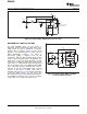
The ADC interface in Figure 64 shows a DC-coupled,
AC-coupling corner), and a maximum stop band
single-supply ADC driver circuit. Many systems are
attenuation of 36dB.
now requiring +3.3V supply capability of both the
ADC and its driver. The OPA2832 provides excellent
performance in this demanding application. Its large
input and output voltage ranges and low distortion
support converters such as the ADS5203. The input
level-shifting circuitry was designed so that V
IN
can
be between 0V and 0.5V, while delivering an output
voltage of 1V to 2V for the ADS5203.
Figure 65. 1MHz, 2nd-Order, Butterworth
Low-Pass Filter
Figure 64. DC-Coupled, +3V ADC Driver
Copyright © 2005 – 2008, Texas Instruments Incorporated Submit Documentation Feedback 21
Product Folder Link(s): OPA2832