
Datasheet


OPA2822
20
SBOS188E
www.ti.com
Inverting operation offers some interesting opportunities to
increase the available signal bandwidth. When the source
impedance is matched by the gain resistor (Figure 10 for
example), the signal gain is (1 + R
F
/R
G
) while the noise gain
is (1 + R
F
/2R
G
). This reduces the noise gain almost by half,
extending the signal bandwidth and increasing the loop gain.
For instance, setting R
F
= 500Ω in Figure 10 will give a signal
gain for the amplifier of 5V/V. However, including the 50Ω
source impedance reflected through the 1:2 transformer will
give an additional 100Ω source impedance for the noise gain
analysis for each of the amplifiers. This reduces the noise gain
to 1 + 500Ω/200Ω = 3.5V/V and results in an amplifier
bandwidth of at least 240MHz/3.5 = 68MHz.
DRIVING CAPACITIVE LOADS
One of the most demanding and yet very common load
conditions for an op amp is capacitive loading. Often, the
capacitive load is the input of an ADC, including additional
external capacitance which may be recommended to im-
prove ADC linearity. A high-speed, high open-loop gain
amplifier like the OPA2822 can be very susceptible to de-
creased stability and closed-loop frequency response peak-
ing when a capacitive load is placed directly on the output
pin. When the amplifier’s open-loop output resistance is
considered, this capacitive load introduces an additional pole
in the signal path that can decrease the phase margin.
Several external solutions to this problem have been sug-
gested. When the primary considerations are frequency
response flatness with low noise and distortion, the simplest
and most effective solution is to isolate the capacitive load
from the feedback loop by inserting a series isolation resistor
between the amplifier output and the capacitive load. This
does not eliminate the pole from the loop response, but
instead shifts it and adds a zero at a higher frequency. The
additional zero acts to cancel the phase lag from the capaci-
tive load pole, thus increasing the phase margin and improv-
ing stability.
The Typical Characteristics show the recommended R
S
ver-
sus capacitive load and the resulting frequency response at
the load. For the OPA2822 operating at a gain of +2, the
frequency response at the output pin is already slightly
peaked without the capacitive load, requiring relatively high
values of R
S
to flatten the response at the load. One way to
reduce the required R
S
value is to use the noise gain
adjustment circuit of Figure 12.
The resistor across the two inputs, R
NG
, can be used to
increase the noise gain while retaining the desired signal
gain. This can be used either to improve flatness at low gains
or to reduce the required value of R
S
in capacitive load
driving applications. This circuit was used with R
NG
adjusted
to produce the gain flatness curve in the Typical Character-
istics. As shown in that curve, an R
NG
of 452Ω will give an NG
of 3 giving exceptional frequency response flatness at a
signal gain of +2. Equation 4 shows the calculation for R
NG
given a target noise gain (NG) and signal gain (G):
R
RRG
NG G
NG
F
S
=
+
−
(4)
where R
S
= Total Source Impedance on the Noninverting
Input [25Ω in Figure 12]
G = Signal Gain [1 + (R
F
/R
G
)]
NG = Noise Gain Target
Using this technique to get initial frequency response flat-
ness will significantly reduce the required series resistor
value to get a flat response at the capacitive load. Using the
best-case noise gain of 3 with a signal gain of 2 allows the
required R
S
to be reduced, as shown in Figure 13. Here, the
required R
S
versus Capacitive Load is replotted along with
data from the Typical Characteristics. This demonstrates that
the use of R
NG
= 452Ω across the inputs results in much
lower required R
S
values to achieve a flat response.
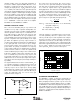
FIGURE 12. Noise Gain Tuning for Noninverting Circuit.
1/2
OPA2822
50Ω
R
G
402Ω
R
NG
R
F
402Ω
50Ω Source
FIGURE 13. Required R
S
vs Noise Gain.
100
10
1
Capacitive Load (pF)
10 100 1000
R
S
(Ω)
NG = 3, R
NG
= 452Ω
NG = 2, R
NG
= ∞
DISTORTION PERFORMANCE
The OPA2822 is capable of delivering exceptionally low
distortion through approximately 5MHz signal frequency.
While principally intended to provide very low noise and
distortion through the maximum ADSL frequency of 1.1MHz,
the OPA2822 in a differential configuration can deliver lower
than –85dBc distortions for a 4V
PP
swing through 5MHz. For
applications requiring extremely low distortion through higher
frequencies, consider higher slew rate amplifiers such as the
OPA687 or OPA2681.