
Datasheet


www.ti.com
DC Accuracy and Offset Control
1/2
OPA2652
4kTR
F
4kTR
S
4kT
R
G
R
G
R
F
R
S
I
BI
E
O
I
BN
4kT=1.6x10 J
-20
at290 K°
E
RS
E
NI
"
ǒ
NG @ V
OS
(
MAX
)
Ǔ
"
ǒ
R
F
@ I
OS
(
MAX
)
Ǔ
+ "
(
1.94 @ 7.0mV
)
"
(
402W @ 1.0mA
)
+ " 14.0mV
ǒ
NG + noninverting signal gain
Ǔ
E
N
+ E
NI
2
)
ǒ
I
BN
R
S
Ǔ
2
)4kTR
S
)
ǒ
I
BI
R
F
NG
Ǔ
2
)
4kTR
F
NG
Ǹ
E
O
+
ǒ
E
NI
2
)
ǒ
I
BN
R
S
Ǔ
2
)4kTR
S
Ǔ
NG
2
)
(
I
BI
R
F
)
2
)4kTR
F
NG
Ǹ
OPA2652
SBOS125A – JUNE 2000 – REVISED MAY 2006
The balanced input stage of a wideband voltage
feedback op amp allows good output DC accuracy in
a wide variety of applications. Although the
high-speed input stage does require relatively high
input bias current (typically 4 µ A out of each input
terminal), the close matching between them may be
used to significantly reduce the output DC error
caused by this current. This reduction is done by
matching the DC source resistances appearing at the
two inputs. This matching reduces the output DC
error resulting from the input bias currents to the
offset current times the feedback resistor. Evaluating
the configuration of Figure 28 , using worst-case
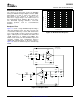
Figure 35. Op Amp Noise Analysis Model
+25 ° C input offset voltage and current specifications,
gives a worst-case output offset voltage equal to:
The total output spot noise voltage can be computed
as the square root of the sum of all squared output
noise voltage contributors. Equation 1 shows the
general form for the output noise voltage using the
terms shown in Figure 35 .
A fine scale output offset null, or DC operating point
adjustment, is often required. Numerous techniques
are available for introducing DC offset control into an
(1)
op amp circuit. Most of these techniques add a DC
current through the feedback resistor. In selecting an
Dividing this expression by the noise gain (NG = 1 +
offset trim method, one key consideration is the
R
F
/R
G
) gives the equivalent input-referred spot noise
impact on the desired signal path frequency
voltage at the noninverting input, as shown in
response. If the signal path is intended to be
Equation 2 .
noninverting, the offset control is best applied as an
inverting summing signal to avoid interaction with the
signal source. If the signal path is intended to be
(2)
inverting, applying the offset control to the
noninverting input may be considered. However, the
Evaluating these two equations for the OPA2652
DC offset voltage on the summing junction sets up a
circuit and component values shown in Figure 28
DC current back into the source which must be
gives a total output spot noise voltage of 17nV/ √ Hz
considered. Applying an offset adjustment to the
and a total equivalent input spot noise voltage of
inverting op amp input can change the noise gain
8.4nV/ √ Hz. This noise includes the noise added by
and frequency response flatness. For a DC-coupled
the bias current cancellation resistor (205 Ω ) on the
inverting amplifier, Figure 36 shows one example of
noninverting input. This total input-referred spot
an offset adjustment technique that has minimal
noise voltage is only slightly higher than the 8nV/ √ Hz
impact on the signal frequency response. In this
specification for the op amp voltage noise alone.
case, the DC offset current is brought into the
This result will be the case as long as the
inverting input node through resistor values that are
impedances appearing at each op amp input are
much larger than the signal path resistors. This
limited to the previously recommend maximum value
configuration ensures that the adjustment circuit has
of 300 Ω . Keeping both (R
F
|| R
G
) and the
minimal effect on the loop gain, and therefore on the
noninverting input source impedance less than 300 Ω
frequency response as well.
satisfies both noise and frequency response flatness
considerations. Since the resistor-induced noise is
relatively negligible, additional capacitive decoupling
across the bias current cancellation resistor (R
B
) for
the inverting op amp configuration of Figure 29 is not
required.
15
Submit Documentation Feedback