
Datasheet


www.ti.com
OPERATING SUGGESTIONS
Optimizing Resistor Values
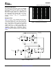
Inverting Amplifier Operation
Bandwidth vs Gain: Noninverting Operation
OPA2652
SBOS125A – JUNE 2000 – REVISED MAY 2006
causes the phase margin to approach 90 ° and the
bandwidth to more closely approach the predicted
value of (GBP/NG). At a gain of +5, the 45MHz
bandwidth shown in the Electrical Characteristics is
Because the OPA2652 is a unity gain stable voltage
close to that predicted using this simple formula.
feedback op amp, a wide range of resistor values
may be used for the feedback and gain setting
resistors. The primary limits on these values are set
by dynamic range (noise and distortion) and parasitic Because the OPA2652 is a general-purpose,
capacitance considerations. For a noninverting unity wideband voltage feedback op amp, all of the
gain follower application, the feedback connection familiar op amp application circuits are available to
should be made with a 25 Ω resistor, not a direct the designer. Inverting operation is one of the more
short. This configuration isolates the inverting input common requirements and offers several
capacitance from the output pin and improves the performance benefits. Figure 29 shows a typical
frequency response flatness. Usually, the feedback inverting configuration.
resistor value should be between 200 Ω and 1.5k Ω .
In the inverting configuration, three key design
Below 200 Ω , the feedback network presents
consideration must be noted. First, the gain resistor
additional output loading that can degrade the
(R
G
) becomes part of the signal channel input
harmonic distortion performance of the OPA2652.
impedance. If input impedance matching is desired
Above 1.5k Ω , the typical parasitic capacitance
(which is beneficial whenever the signal is coupled
(approximately 0.2pF) across the feedback resistor
through a cable, twisted pair, long PCB trace or other
may cause unintentional bandlimiting in the amplifier
transmission line conductor), R
G
may be set equal to
response.
the required termination value and R
F
adjusted to
A good rule of thumb is to target the parallel give the desired gain. This approach is the simplest,
combination of R
F
and R
G
(see Figure 28 ) to be less and results in optimum bandwidth and noise
than approximately 300 Ω . The combined impedance performance. However, at low inverting gains, the
R
F
|| R
G
interacts with the inverting input resulting feedback resistor value can present a
capacitance, placing an additional pole in the significant load to the amplifier output. For an
feedback network, and thus a zero in the forward inverting gain of –1, setting R
G
to 50 Ω for input
response. Assuming a 2pF total parasitic on the matching eliminates the need for R
M
but requires a
inverting node, holding R
F
|| R
G
< 300 Ω keeps this 50
W
feedback resistor. This configuration has the
pole above 250MHz. By itself, this constraint implies interesting advantage that the noise gain becomes
that the feedback resistor R
F
can increase to several equal to 2 for a 50 Ω source impedance—the same
k Ω at high gains. This increase is acceptable as long as the noninverting circuits considered above.
as the pole formed by R
F
and any parasitic However, the amplifier output now sees the 50 Ω
capacitance appearing in parallel is kept out of the feedback resistor in parallel with the external load. In
frequency range of interest. general, the feedback resistor should be limited to
the 200 Ω to 1.5k Ω range. In this case, it is preferable
to increase both the R
F
and R
G
values as shown in
Figure 29 , and then achieve the input matching
Voltage feedback op amps exhibit decreasing
impedance with a third resistor (R
M
) to ground. The
closed-loop bandwidth as the signal gain is
total input impedance becomes the parallel
increased. In theory, this relationship is described by
combination of R
G
and R
M
.
the Gain Bandwidth Product (GBP) shown in the
specifications. Ideally, dividing GBP by the The second major consideration, touched on in the
noninverting signal gain (also called the Noise Gain, previous paragraph, is that the signal source
or NG) predicts the closed-loop bandwidth. In impedance becomes part of the noise gain equation
practice, this prediction only holds true when the and influences the bandwidth. For the example in
phase margin approaches 90 ° , as it does in high Figure 29 , the R
M
value combines in parallel with the
gain configurations. At low gains (increased external 50 Ω source impedance, yielding an effective
feedback factor), most amplifiers exhibit a wider driving impedance of 50 Ω || 57.6 Ω = 26.8 Ω . This
bandwidth and lower phase margin. The OPA2652 is impedance is added in series with R
G
for calculating
compensated to give a flat response in a the noise gain (NG). The resulting NG is 1.94 for
noninverting gain of 1 (see Figure 28 ). This Figure 29 (an ideal source would cause NG = 2.00).
configuration results in a typical gain of +1 bandwidth
The third important consideration in inverting
of 700MHz, far exceeding that predicted by dividing
amplifier design is setting the bias current
the 200MHz GBP by NG = 1. Increasing the gain
cancellation resistor on the noninverting input (R
B
). If
this resistor is set equal to the total DC resistance
looking out of the inverting node, the output DC
13
Submit Documentation Feedback