
Datasheet


"#$
%"#$
$"#$
SBOS233E − MARCH 2002− REVISED MAY 2009
www.ti.com
4
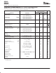
ELECTRICAL CHARACTERISTICS: V
S
= +2.7V to +5.5V Single-Supply
Boldface limits apply over the specified temperature range, T
A
= −40°C to +125°C.
At T
A
= +25°C, R
F
= 0Ω , R
L
= 1kΩ, and connected to V
S
/2, unless otherwise noted.
OPA354AI
OPA2354AI, OPA4354AI
PARAMETER CONDITIONS MIN TYP MAX UNITS
OFFSET VOLTAGE
Input Offset Voltage V
OS
V
S
= +5V ±2 ±8 mV
Specified Temperature Range +10 mV
vs Temperature dV
OS
/dT Specified Temperature Range +4 µV/°C
vs Power Supply PSRR V
S
= +2.7V to +5.5V, V
CM
= (V
S
/2) − 0.55V ±200 ±800 µV/V
Specified Temperature Range ±900 µV/V
INPUT BIAS CURRENT
Input Bias Current I
B
3 ±50 pA
Input Offset Current I
OS
±1 ±50 pA
NOISE
Input Voltage Noise Density e
n
f = 1MHz 6.5 nV/√Hz
Current Noise Density i
n
f = 1MHz 50 fA/√Hz
INPUT VOLTAGE RANGE
Common-Mode Voltage Range V
CM
(V−) − 0.1 (V+) + 0.1 V
Common-Mode Rejection Ratio CMRR V
S
= +5.5V, −0.1V < V
CM
< +3.5V 66 80 dB
Specified Temperature Range 64 dB
V
S
= +5.5V, −0.1V < V
CM
< +5.6V 56 68 dB
Specified Temperature Range 55 dB
INPUT IMPEDANCE
Differential 10
13
|| 2 Ω || pF
Common-Mode 10
13
|| 2 Ω || pF
OPEN-LOOP GAIN A
OL
V
S
= +5V, +0.3V < V
O
< +4.7V 94 110 dB
Specified Temperature Range V
S
= +5V, +0.4V < V
O
< +4.6V 90 dB
FREQUENCY RESPONSE
Small-Signal Bandwidth f
−3dB
G = +1, V
O
= 100mV
PP
, R
F
= 25Ω 250 MHz
f
−3dB
G = +2, V
O
= 100mV
PP
90 MHz
Gain-Bandwidth Product GBW G = +10 100 MHz
Bandwidth for 0.1dB Gain Flatness f
0.1dB
G = +2, V
O
= 100mV
PP
40 MHz
Slew Rate SR V
S
= +5V, G = +1, 4V Step 150 V/µs
V
S
= +5V, G = +1, 2V Step 130 V/µs
V
S
= +3V, G = +1, 2V Step 110 V/µs
Rise-and-Fall Time G = +1, V
O
= 200mV
PP
, 10% to 90% 2 ns
G = +1, V
O
= 2V
PP
, 10% to 90% 11 ns
Settling Time, 0.1% V
S
= +5V, G = +1, 2V Output Step 30 ns
0.01% 60 ns
Overload Recovery Time V
IN
S Gain = V
S
5 ns
Harmonic Distortion
2nd-Harmonic G = +1, f = 1MHz, V
O
= 2V
PP
, R
L
= 200Ω, V
CM
= 1.5V −75 dBc
3rd-Harmonic G = +1, f = 1MHz, V
O
= 2V
PP
, R
L
= 200Ω, V
CM
= 1.5V −83 dBc
Differential Gain Error NTSC, R
L
= 150Ω 0.02 %
Differential Phase Error NTSC, R
L
= 150Ω 0.09 degrees
Channel-to-Channel Crosstalk
OPA2354 f = 5MHz −100 dB
OPA4354 −84 dB
(1)
See typical characteristics Output Voltage Swing vs Output Current.
(2)
Specified by design.