
Datasheet


P3.0/TA0.2
P3.1/TA1.0
P3.2/TA1.1
P3.3/TA1.2
P3.4/TA0.0
P3.5/TA0.1
P3.6/TA0.2
P3.7/TA1CLK/CAOUT
Direction
0: Input
1: Output
To Module
From Module
PxOUT.y
DVSS
DVCC
1
TAx.y
TAxCLK
1
0
PxIN.y
EN
D
PxSEL.y
PxREN.y
1
0
PxDIR.y
1
0
PxSEL2.y
PxSEL.y
1
0
PxSEL.y
1
3
2
1
0
PxSEL2.y
MSP430G2x33
MSP430G2x03
www.ti.com
SLAS734F –APRIL 2011–REVISED MAY 2013
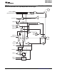
Port P3 Pin Schematic: P3.0 to P3.7, Input/Output With Schmitt Trigger (RHB Package Only)
Copyright © 2011–2013, Texas Instruments Incorporated Submit Documentation Feedback 53