
Datasheet


MSP430G2x32
MSP430G2x02
SLAS723H –DECEMBER 2010–REVISED MAY 2013
www.ti.com
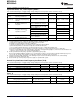
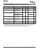
10-Bit ADC, Power Supply and Input Range Conditions (MSP430G2x32 Only)
over recommended ranges of supply voltage and operating free-air temperature (unless otherwise noted)
(1)
PARAMETER TEST CONDITIONS T
A
V
CC
MIN TYP MAX UNIT
V
CC
Analog supply voltage V
SS
= 0 V 2.2 3.6 V
All Ax terminals, Analog inputs
V
Ax
Analog input voltage
(2)
3 V 0 V
CC
V
selected in ADC10AE register
f
ADC10CLK
= 5.0 MHz,
ADC10ON = 1, REFON = 0,
I
ADC10
ADC10 supply current
(3)
25°C 3 V 0.6 mA
ADC10SHT0 = 1, ADC10SHT1 = 0,
ADC10DIV = 0
f
ADC10CLK
= 5.0 MHz,
ADC10ON = 0, REF2_5V = 0, 0.25
REFON = 1, REFOUT = 0
Reference supply current,
I
REF+
25°C 3 V mA
reference buffer disabled
(4)
f
ADC10CLK
= 5.0 MHz,
ADC10ON = 0, REF2_5V = 1, 0.25
REFON = 1, REFOUT = 0
f
ADC10CLK
= 5.0 MHz,
Reference buffer supply ADC10ON = 0, REFON = 1,
I
REFB,0
25°C 3 V 1.1 mA
current with ADC10SR = 0
(4)
REF2_5V = 0, REFOUT = 1,
ADC10SR = 0
f
ADC10CLK
= 5.0 MHz,
Reference buffer supply ADC10ON = 0, REFON = 1,
I
REFB,1
25°C 3 V 0.5 mA
current with ADC10SR = 1
(4)
REF2_5V = 0, REFOUT = 1,
ADC10SR = 1
Only one terminal Ax can be selected
C
I
Input capacitance 25°C 3 V 27 pF
at one time
R
I
Input MUX ON resistance 0 V ≤ V
Ax
≤ V
CC
25°C 3 V 1000 Ω
(1) The leakage current is defined in the leakage current table with Px.x/Ax parameter.
(2) The analog input voltage range must be within the selected reference voltage range V
R+
to V
R–
for valid conversion results.
(3) The internal reference supply current is not included in current consumption parameter I
ADC10
.
(4) The internal reference current is supplied via terminal V
CC
. Consumption is independent of the ADC10ON control bit, unless a
conversion is active. The REFON bit enables the built-in reference to settle before starting an A/D conversion.
30 Submit Documentation Feedback Copyright © 2010–2013, Texas Instruments Incorporated