MSP430G2x31 MSP430G2x21 www.ti.com SLAS694J – FEBRUARY 2010 – REVISED FEBRUARY 2013 MIXED SIGNAL MICROCONTROLLER FEATURES 1 • • • • • • Low Supply-Voltage Range: 1.8 V to 3.6 V Ultra-Low Power Consumption – Active Mode: 220 µA at 1 MHz, 2.2 V – Standby Mode: 0.5 µA – Off Mode (RAM Retention): 0.1 µA Five Power-Saving Modes Ultra-Fast Wake-Up From Standby Mode in Less Than 1 µs 16-Bit RISC Architecture, 62.
MSP430G2x31 MSP430G2x21 SLAS694J – FEBRUARY 2010 – REVISED FEBRUARY 2013 www.ti.com Table 1.
MSP430G2x31 MSP430G2x21 www.ti.com SLAS694J – FEBRUARY 2010 – REVISED FEBRUARY 2013 Device Pinout, MSP430G2x21 N OR PW PACKAGE (TOP VIEW) DVCC P1.0/TA0CLK/ACLK 1 14 2 13 P1.1/TA0.0 P1.2/TA0.1 P1.3 P1.4/SMCLK/TCK 3 12 4 11 5 10 6 9 P1.5/TA0.0/SCLK/TMS 7 8 DVSS XIN/P2.6/TA0.1 XOUT/P2.7 TEST/SBWTCK RST/NMI/SBWTDIO P1.7/SDI/SDA/TDO/TDI P1.6/TA0.1/SDO/SCL/TDI/TCLK NOTE: See port schematics in Application Information for detailed I/O information.
MSP430G2x31 MSP430G2x21 SLAS694J – FEBRUARY 2010 – REVISED FEBRUARY 2013 www.ti.com Device Pinout, MSP430G2x31 N OR PW PACKAGE (TOP VIEW) DVCC P1.0/TA0CLK/ACLK/A0 1 14 2 13 P1.1/TA0.0/A1 P1.2/TA0.1/A2 P1.3/ADC10CLK/A3/VREF-/VEREFP1.4/SMCLK/A4/VREF+/VEREF+/TCK 3 12 4 11 5 10 6 9 P1.5/TA0.0/A5/SCLK/TMS 7 8 DVSS XIN/P2.6/TA0.1 XOUT/P2.7 TEST/SBWTCK RST/NMI/SBWTDIO P1.7/A7/SDI/SDA/TDO/TDI P1.6/TA0.
MSP430G2x31 MSP430G2x21 www.ti.com SLAS694J – FEBRUARY 2010 – REVISED FEBRUARY 2013 Functional Block Diagram, MSP430G2x21 DVCC XIN XOUT DVSS P1.x P2.x 8 2 Port P1 Port P2 8 I/O Interrupt capability pull-up/down resistors 2 I/O Interrupt capability pull-up/down resistors ACLK Clock System SMCLK Flash 2KB 1KB MCLK 16MHz CPU MAB incl.
MSP430G2x31 MSP430G2x21 SLAS694J – FEBRUARY 2010 – REVISED FEBRUARY 2013 www.ti.com Table 2. Terminal Functions TERMINAL NAME NO. I/O DESCRIPTION N, PW RSA P1.0/ TA0CLK/ ACLK/ A0 2 1 I/O General-purpose digital I/O pin Timer0_A, clock signal TACLK input ACLK signal output ADC10 analog input A0 (1) P1.1/ TA0.0/ A1 3 2 I/O General-purpose digital I/O pin Timer0_A, capture: CCI0A input, compare: Out0 output ADC10 analog input A1 (1) P1.2/ TA0.
MSP430G2x31 MSP430G2x21 www.ti.com SLAS694J – FEBRUARY 2010 – REVISED FEBRUARY 2013 SHORT-FORM DESCRIPTION CPU The MSP430 CPU has a 16-bit RISC architecture that is highly transparent to the application. All operations, other than program-flow instructions, are performed as register operations in conjunction with seven addressing modes for source operand and four addressing modes for destination operand.
MSP430G2x31 MSP430G2x21 SLAS694J – FEBRUARY 2010 – REVISED FEBRUARY 2013 www.ti.com Operating Modes The MSP430 has one active mode and five software selectable low-power modes of operation. An interrupt event can wake up the device from any of the low-power modes, service the request, and restore back to the low-power mode on return from the interrupt program.
MSP430G2x31 MSP430G2x21 www.ti.com SLAS694J – FEBRUARY 2010 – REVISED FEBRUARY 2013 Interrupt Vector Addresses The interrupt vectors and the power-up starting address are located in the address range 0FFFFh to 0FFC0h. The vector contains the 16-bit address of the appropriate interrupt handler instruction sequence. If the reset vector (located at address 0FFFEh) contains 0FFFFh (for example, flash is not programmed) the CPU goes into LPM4 immediately after power-up. Table 5.
MSP430G2x31 MSP430G2x21 SLAS694J – FEBRUARY 2010 – REVISED FEBRUARY 2013 www.ti.com Special Function Registers (SFRs) Most interrupt and module enable bits are collected into the lowest address space. Special function register bits not allocated to a functional purpose are not physically present in the device. Simple software access is provided with this arrangement. Legend rw: rw-0,1: rw-(0,1): Bit can be read and written. Bit can be read and written. It is reset or set by PUC.
MSP430G2x31 MSP430G2x21 www.ti.com SLAS694J – FEBRUARY 2010 – REVISED FEBRUARY 2013 Memory Organization Table 8.
MSP430G2x31 MSP430G2x21 SLAS694J – FEBRUARY 2010 – REVISED FEBRUARY 2013 www.ti.com Peripherals Peripherals are connected to the CPU through data, address, and control buses and can be handled using all instructions. For complete module descriptions, see the MSP430x2xx Family User's Guide (SLAU144).
MSP430G2x31 MSP430G2x21 www.ti.com SLAS694J – FEBRUARY 2010 – REVISED FEBRUARY 2013 Timer_A2 Timer_A2 is a 16-bit timer/counter with two capture/compare registers. Timer_A2 can support multiple capture/compares, PWM outputs, and interval timing. Timer_A2 also has extensive interrupt capabilities. Interrupts may be generated from the counter on overflow conditions and from each of the capture/compare registers. Table 10.
MSP430G2x31 MSP430G2x21 SLAS694J – FEBRUARY 2010 – REVISED FEBRUARY 2013 www.ti.com Peripheral File Map Table 11.
MSP430G2x31 MSP430G2x21 www.ti.com SLAS694J – FEBRUARY 2010 – REVISED FEBRUARY 2013 Table 12.
MSP430G2x31 MSP430G2x21 SLAS694J – FEBRUARY 2010 – REVISED FEBRUARY 2013 www.ti.com Absolute Maximum Ratings (1) Voltage applied at VCC to VSS –0.3 V to 4.1 V Voltage applied to any pin (2) –0.3 V to VCC + 0.3 V Diode current at any device pin Storage temperature range, Tstg (1) ±2 mA (3) Unprogrammed device –55°C to 150°C Programmed device –55°C to 150°C Stresses beyond those listed under "absolute maximum ratings" may cause permanent damage to the device.
MSP430G2x31 MSP430G2x21 www.ti.
MSP430G2x31 MSP430G2x21 SLAS694J – FEBRUARY 2010 – REVISED FEBRUARY 2013 www.ti.com Low-Power Mode Supply Currents (Into VCC) Excluding External Current over recommended ranges of supply voltage and operating free-air temperature (unless otherwise noted) (1) PARAMETER TA VCC Low-power mode 0 (LPM0) current (3) fMCLK = 0 MHz, fSMCLK = fDCO = 1 MHz, fACLK = 32768 Hz, BCSCTL1 = CALBC1_1MHZ, DCOCTL = CALDCO_1MHZ, CPUOFF = 1, SCG0 = 0, SCG1 = 0, OSCOFF = 0 25°C 2.
MSP430G2x31 MSP430G2x21 www.ti.com SLAS694J – FEBRUARY 2010 – REVISED FEBRUARY 2013 Schmitt-Trigger Inputs – Ports Px over recommended ranges of supply voltage and operating free-air temperature (unless otherwise noted) PARAMETER TEST CONDITIONS VIT+ Positive-going input threshold voltage VIT– Negative-going input threshold voltage Vhys Input voltage hysteresis (VIT+ – VIT–) VCC MIN RPull Pullup/pulldown resistor CI Input capacitance VIN = VSS or VCC MAX 0.45 VCC 0.75 VCC 1.35 2.
MSP430G2x31 MSP430G2x21 SLAS694J – FEBRUARY 2010 – REVISED FEBRUARY 2013 www.ti.com Typical Characteristics – Outputs over recommended ranges of supply voltage and operating free-air temperature (unless otherwise noted) TYPICAL LOW-LEVEL OUTPUT CURRENT vs LOW-LEVEL OUTPUT VOLTAGE TYPICAL LOW-LEVEL OUTPUT CURRENT vs LOW-LEVEL OUTPUT VOLTAGE 50 VCC = 2.2 V P1.7 TA = 25°C 25 TA = 85°C 20 15 10 5 I OL − Typical Low-Level Output Current − mA I OL − Typical Low-Level Output Current − mA 30 0 0.
MSP430G2x31 MSP430G2x21 www.ti.com SLAS694J – FEBRUARY 2010 – REVISED FEBRUARY 2013 POR, BOR (1) (2) over recommended ranges of supply voltage and operating free-air temperature (unless otherwise noted) PARAMETER TEST CONDITIONS VCC MIN TYP MAX UNIT VCC(start) See Figure 10 dVCC/dt ≤ 3 V/s V(B_IT–) See Figure 10 through Figure 12 dVCC/dt ≤ 3 V/s 1.
MSP430G2x31 MSP430G2x21 SLAS694J – FEBRUARY 2010 – REVISED FEBRUARY 2013 www.ti.com Typical Characteristics – POR and BOR VCC 3V 2 VCC(drop) − V VCC = 3 V Typical Conditions t pw 1.5 1 VCC(drop) 0.5 0 0.001 1 1000 1 ns 1 ns t pw − Pulse Width − µs t pw − Pulse Width − µs Figure 11. VCC(drop) Level With a Square Voltage Drop to Generate a POR or BOR Signal VCC 2 t pw 3V VCC(drop) − V VCC = 3 V 1.5 Typical Conditions 1 VCC(drop) 0.5 0 0.
MSP430G2x31 MSP430G2x21 www.ti.com SLAS694J – FEBRUARY 2010 – REVISED FEBRUARY 2013 Main DCO Characteristics • • • All ranges selected by RSELx overlap with RSELx + 1: RSELx = 0 overlaps RSELx = 1, ... RSELx = 14 overlaps RSELx = 15. DCO control bits DCOx have a step size as defined by parameter SDCO. Modulation control bits MODx select how often fDCO(RSEL,DCO+1) is used within the period of 32 DCOCLK cycles. The frequency fDCO(RSEL,DCO) is used for the remaining cycles.
MSP430G2x31 MSP430G2x21 SLAS694J – FEBRUARY 2010 – REVISED FEBRUARY 2013 www.ti.com Calibrated DCO Frequencies – Tolerance over recommended ranges of supply voltage and operating free-air temperature (unless otherwise noted) PARAMETER TEST CONDITIONS TA VCC MIN TYP MAX UNIT 1-MHz tolerance over temperature (1) BCSCTL1= CALBC1_1MHz, DCOCTL = CALDCO_1MHz, calibrated at 30°C and 3 V 0°C to 85°C 3V -3 ±0.
MSP430G2x31 MSP430G2x21 www.ti.
MSP430G2x31 MSP430G2x21 SLAS694J – FEBRUARY 2010 – REVISED FEBRUARY 2013 www.ti.com USI, Universal Serial Interface over recommended ranges of supply voltage and operating free-air temperature (unless otherwise noted) PARAMETER TEST CONDITIONS fUSI USI clock frequency External: SCLK, Duty cycle = 50% ±10%, SPI slave mode VOL,I2C Low-level output voltage on SDA and SCL USI module in I2C mode, I(OLmax) = 1.5 mA VCC MIN TYP MAX fSYSTEM 3V UNIT MHz VSS + 0.
MSP430G2x31 MSP430G2x21 www.ti.
MSP430G2x31 MSP430G2x21 SLAS694J – FEBRUARY 2010 – REVISED FEBRUARY 2013 www.ti.
MSP430G2x31 MSP430G2x21 www.ti.com SLAS694J – FEBRUARY 2010 – REVISED FEBRUARY 2013 10-Bit ADC, External Reference (1) (MSP430G2x31 Only) over recommended ranges of supply voltage and operating free-air temperature (unless otherwise noted) PARAMETER VEREF+ TEST CONDITIONS Positive external reference input voltage range (2) 1.4 3 0 1.2 V 1.4 VCC V Differential external reference input voltage range, ΔVEREF = VEREF+ – VEREF– VEREF+ > VEREF– (1) (2) (3) (4) (5) UNIT VEREF– ≤ VEREF+ ≤ VCC – 0.
MSP430G2x31 MSP430G2x21 SLAS694J – FEBRUARY 2010 – REVISED FEBRUARY 2013 www.ti.com 10-Bit ADC, Temperature Sensor and Built-In VMID (MSP430G2x31 Only) over recommended ranges of supply voltage and operating free-air temperature (unless otherwise noted) PARAMETER ISENSOR TEST CONDITIONS Temperature sensor supply current (1) TCSENSOR VCC REFON = 0, INCHx = 0Ah, TA = 25°C ADC10ON = 1, INCHx = 0Ah (2) 60 3V 3.
MSP430G2x31 MSP430G2x21 www.ti.com SLAS694J – FEBRUARY 2010 – REVISED FEBRUARY 2013 RAM over recommended ranges of supply voltage and operating free-air temperature (unless otherwise noted) PARAMETER V(RAMh) (1) RAM retention supply voltage TEST CONDITIONS (1) MIN CPU halted MAX UNIT 1.6 V This parameter defines the minimum supply voltage VCC when the data in RAM remains unchanged. No program execution should happen during this supply voltage condition.
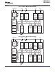
MSP430G2x31 MSP430G2x21 SLAS694J – FEBRUARY 2010 – REVISED FEBRUARY 2013 www.ti.com APPLICATION INFORMATION Port P1 Pin Schematic: P1.0 to P1.3, Input/Output With Schmitt Trigger – MSP430G2x21 PxSEL.y PxDIR.y 1 Direction 0: Input 1: Output 0 PxREN.y PxSEL.y PxOUT.y 0 From Timer 1 DVSS 0 DVCC 1 1 P1.0/TA0CLK/ACLK P1.1/TA0.0 P1.2/TA0.1 P1.3 PxIN.y To Module PxIE.y PxIRQ.y EN Q Set PxIFG.y Interrupt Edge Select PxSEL.y PxIES.y Table 13. Port P1 (P1.0 to P1.
MSP430G2x31 MSP430G2x21 www.ti.com SLAS694J – FEBRUARY 2010 – REVISED FEBRUARY 2013 Port P1 Pin Schematic: P1.4, Input/Output With Schmitt Trigger – MSP430G2x21 PxSEL.y PxDIR.y 1 Direction 0: Input 1: Output 0 PxREN.y PxSEL.y PxOUT.y DVSS 0 DVCC 1 1 0 From Module 1 P1.4/SMCLK/TCK PxIN.y To Module PxIE.y PxIRQ.y EN Q Set PxIFG.y Interrupt Edge Select PxSEL.y PxIES.y From JTAG To JTAG Table 14. Port P1 (P1.4) Pin Functions – MSP430G2x21 PIN NAME (P1.x) x P1.
MSP430G2x31 MSP430G2x21 SLAS694J – FEBRUARY 2010 – REVISED FEBRUARY 2013 www.ti.com Port P1 Pin Schematic: P1.5, Input/Output With Schmitt Trigger – MSP430G2x21 PxSEL.y PxDIR.y 1 From USI Direction 0: Input 1: Output 0 PxREN.y PxSEL.y or USIPE5 PxOUT.y DVSS 0 DV CC 1 1 0 From USI 1 P1.5/TA0.0/SCLK/TMS PxSEL.y PxIN.y To Module PxIE.y PxIRQ.y EN Q Set PxIFG.y Interrupt Edge Select PxSEL.y PxIES.y From JTAG To JTAG Table 15. Port P1 (P1.5) Pin Functions – MSP430G2x21 PIN NAME (P1.
MSP430G2x31 MSP430G2x21 www.ti.com SLAS694J – FEBRUARY 2010 – REVISED FEBRUARY 2013 Port P1 Pin Schematic: P1.6, Input/Output With Schmitt Trigger – MSP430G2x21 PxSEL.y PxDIR.y 1 Direction 0: Input 1: Output 0 PxREN.y PxSEL.y or USIPE6 PxOUT.y DVSS 0 DV CC 1 1 0 From Module 1 P1.6/TA0.1/SDO/SCL/TDI PxSEL.y PxIN.y To Module PxIE.y PxIRQ.y EN Q Set PxIFG.y Interrupt Edge Select PxSEL.y PxIES.y From JTAG To JTAG Table 16. Port P1 (P1.6) Pin Functions – MSP430G2x21 PIN NAME (P1.
MSP430G2x31 MSP430G2x21 SLAS694J – FEBRUARY 2010 – REVISED FEBRUARY 2013 www.ti.com Port P1 Pin Schematic: P1.7, Input/Output With Schmitt Trigger – MSP430G2x21 USIPE7 PxDIR.y From USI 1 Direction 0: Input 1: Output 0 PxREN.y PxSEL.y or USIPE7 PxOUT.y DVSS 0 DVCC 1 1 0 From USI 1 P1.7/SDI/SDA/TDO/TDI PxSEL.y PxIN.y To Module PxIE.y PxIRQ.y EN Q Set PxIFG.y Interrupt Edge Select PxSEL.y PxIES.y From JTAG To JTAG From JTAG To JTAG Table 17. Port P1 (P1.
MSP430G2x31 MSP430G2x21 www.ti.com SLAS694J – FEBRUARY 2010 – REVISED FEBRUARY 2013 Port P1 Pin Schematic: P1.0 to P1.2, Input/Output With Schmitt Trigger – MSP430G2x31 To ADC10 INCHx ADC10AE0.y PxSEL.y PxDIR.y 1 Direction 0: Input 1: Output 0 PxREN.y PxSEL.y PxOUT.y 0 ACLK 1 DVSS 0 DVCC 1 1 P1.0/TA0CLK/ACLK/A0 P1.1/TA0.0/A1 P1.2/TA0.1/A2 Bus Keeper EN PxIN.y To Module PxIE.y PxIRQ.y EN Q Set PxIFG.y Interrupt Edge Select PxSEL.y PxIES.y Table 18. Port P1 (P1.0 to P1.
MSP430G2x31 MSP430G2x21 SLAS694J – FEBRUARY 2010 – REVISED FEBRUARY 2013 www.ti.com Port P1 Pin Schematic: P1.3, Input/Output With Schmitt Trigger – MSP430G2x31 SREF2 VSS 0 To ADC10 VREF- 1 To ADC10 INCHx = y ADC10AE0.y PxSEL.y PxDIR.y 1 Direction 0: Input 1: Output 0 PxREN.y PxSEL.y PxOUT.y 0 ADC10CLK 1 DVSS 0 DVCC 1 Bus Keeper EN 1 P1.3/ADC10CLK/A3/VREF-/VEREF- PxIN.y EN To Module D PxIE.y PxIRQ.y EN Q Set PxIFG.y Interrupt Edge Select PxSEL.y PxIES.y Table 19. Port P1 (P1.
MSP430G2x31 MSP430G2x21 www.ti.com SLAS694J – FEBRUARY 2010 – REVISED FEBRUARY 2013 Port P1 Pin Schematic: P1.4, Input/Output With Schmitt Trigger – MSP430G2x31 To ADC10 VREF+ To ADC10 INCHx = y ADC10AE0.y PxSEL.y PxDIR.y 1 Direction 0: Input 1: Output 0 PxREN.y PxSEL.y PxOUT.y 0 SMCLK 1 DVSS 0 DV CC 1 Bus Keeper EN 1 P1.4/SMCLK/A4/VREF+/VEREF+/TCK PxIN.y To Module PxIE.y EN PxIRQ.y Q Set PxIFG.y PxSEL.y PxIES.
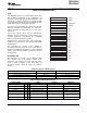
MSP430G2x31 MSP430G2x21 SLAS694J – FEBRUARY 2010 – REVISED FEBRUARY 2013 www.ti.com Table 20. Port P1 (P1.4) Pin Functions – MSP430G2x31 CONTROL BITS / SIGNALS (1) PIN NAME (P1.x) x FUNCTION P1DIR.x P1SEL.x ADC10AE.x (INCH.x = 1) JTAG Mode P1.4/ P1.x (I/O) I: 0; O: 1 0 0 0 SMCLK/ SMCLK 1 1 0 0 A4/ A4 X X 1 (y = 4) 0 4 VREF+/ VREF+ X X 1 0 VEREF+/ VEREF+ X X 1 0 TCK TCK X X 0 1 (1) X = don't care Port P1 Pin Schematic: P1.
MSP430G2x31 MSP430G2x21 www.ti.com SLAS694J – FEBRUARY 2010 – REVISED FEBRUARY 2013 Table 21. Port P1 (P1.5) Pin Functions - MSP430G2x31 CONTROL BITS / SIGNALS (1) PIN NAME (P1.x) x FUNCTION P1DIR.x P1SEL.x USIP.x ADC10AE.x (INCH.x = 1) JTAG Mode P1.5/ P1.x (I/O) I: 0; O: 1 0 0 0 0 TA0.0/ TA0.0 1 1 0 0 0 A5 X X X 1 (y = 5) 0 SCLK/ SCLK X X 1 0 0 TMS TMS X X 0 0 1 A5/ (1) 5 X = don't care Port P1 Pin Schematic: P1.
MSP430G2x31 MSP430G2x21 SLAS694J – FEBRUARY 2010 – REVISED FEBRUARY 2013 www.ti.com Table 22. Port P1 (P1.6) Pin Functions - MSP430G2x31 CONTROL BITS / SIGNALS (1) PIN NAME (P1.x) x FUNCTION P1DIR.x P1SEL.x USIP.x ADC10AE.x (INCH.x = 1) JTAG Mode P1.6/ P1.x (I/O) I: 0; O: 1 0 0 0 0 TA0.1/ TA0.1 1 1 0 0 0 TA0.
MSP430G2x31 MSP430G2x21 www.ti.com SLAS694J – FEBRUARY 2010 – REVISED FEBRUARY 2013 Port P1 Pin Schematic: P1.7, Input/Output With Schmitt Trigger – MSP430G2x31 To ADC10 INCHx ADC10AE0.y USIPE7 PxDIR.y 1 Direction 0: Input 1: Output 0 from USI PxSEL.y PxREN.y PxSEL.y or USIPE7 PxOUT.y 0 From USI 1 DVSS 0 DVCC 1 1 Bus Keeper EN P1.7/SDI/SDA/A7/TDO/TDI PxSEL.y PxIN.y To Module PxIE.y EN PxIRQ.y Q Set PxIFG.y Interrupt Edge Select PxSEL.y PxIES.
MSP430G2x31 MSP430G2x21 SLAS694J – FEBRUARY 2010 – REVISED FEBRUARY 2013 www.ti.com Port P2 Pin Schematic: P2.6, Input/Output With Schmitt Trigger – MSP430G2x21 and MSP430G2x31 XOUT/P2.7 LF off PxSEL.6 PxSEL.7 BCSCTL3.LFXT1Sx = 11 LFXT1CLK 0 1 PxSEL.6 PxDIR.y 1 0 Direction 0: Input 1: Output PxREN.y PxSEL.6 PxOUT.y 0 from Module 1 DV SS 0 DV CC 1 1 Bus Keeper EN XIN/P2.6/TA0.1 PxIN.y To Module PxIE.y PxIRQ.y EN Q Set PxIFG.y PxSEL.y PxIES.y Interrupt Edge Select Table 24.
MSP430G2x31 MSP430G2x21 www.ti.com SLAS694J – FEBRUARY 2010 – REVISED FEBRUARY 2013 Port P2 Pin Schematic: P2.7, Input/Output With Schmitt Trigger – MSP430G2x21 and MSP430G2x31 XIN/P2.6/TA0.1 LF off PxSEL.6 PxSEL.7 BCSCTL3.LFXT1Sx = 11 LFXT1CLK 0 PxSEL.7 PxDIR.y from P2.6/XIN 1 1 Direction 0: Input 1: Output 0 PxREN.y PxSEL.7 PxOUT.y 0 from Module 1 DVSS 0 DV CC 1 1 Bus Keeper EN XOUT/P2.7 PxIN.y To Module PxIE.y PxIRQ.y EN Q Set PxIFG.y Interrupt Edge Select PxSEL.y PxIES.
MSP430G2x31 MSP430G2x21 SLAS694J – FEBRUARY 2010 – REVISED FEBRUARY 2013 www.ti.com REVISION HISTORY REVISION SLAS694 46 DESCRIPTION Limited Product Preview release SLAS694A Updated Product Preview release. Changes throughout for sampling. SLAS694B Updated Product Preview release SLAS694C Production Data release SLAS694D Updated Table 12, Table 15, Table 16, Table 17, Table 19, Table 20, Table 21, Table 24, Table 25. Updated MSP430G2x31 port schematics: P1.0 to P1.3, P1.5, P1.6, P1.7.
PACKAGE OPTION ADDENDUM www.ti.
PACKAGE OPTION ADDENDUM www.ti.
PACKAGE OPTION ADDENDUM www.ti.
PACKAGE MATERIALS INFORMATION www.ti.com 9-Oct-2013 TAPE AND REEL INFORMATION *All dimensions are nominal Device Package Package Pins Type Drawing MSP430G2121IPW14R TSSOP SPQ Reel Reel A0 Diameter Width (mm) (mm) W1 (mm) PW 14 2000 330.0 12.4 6.9 B0 (mm) K0 (mm) P1 (mm) W Pin1 (mm) Quadrant 5.6 1.6 8.0 12.0 Q1 MSP430G2121IPW14R TSSOP PW 14 2000 330.0 12.4 6.9 5.6 1.6 8.0 12.0 Q1 MSP430G2121IRSA16R QFN RSA 16 3000 330.0 12.4 4.25 4.25 1.15 8.0 12.
PACKAGE MATERIALS INFORMATION www.ti.com 9-Oct-2013 *All dimensions are nominal Device Package Type Package Drawing Pins SPQ Length (mm) Width (mm) Height (mm) MSP430G2121IPW14R TSSOP PW 14 2000 367.0 367.0 35.0 MSP430G2121IPW14R TSSOP PW 14 2000 367.0 367.0 35.0 MSP430G2121IRSA16R QFN RSA 16 3000 367.0 367.0 35.0 MSP430G2121IRSA16T QFN RSA 16 250 210.0 185.0 35.0 MSP430G2131IPW14R TSSOP PW 14 2000 367.0 367.0 35.
IMPORTANT NOTICE Texas Instruments Incorporated and its subsidiaries (TI) reserve the right to make corrections, enhancements, improvements and other changes to its semiconductor products and services per JESD46, latest issue, and to discontinue any product or service per JESD48, latest issue. Buyers should obtain the latest relevant information before placing orders and should verify that such information is current and complete.