
Datasheet


P2.5/TB0.0/UCA1TXD/UCA1SIMO
P2.6/TB1.0/UCA1RXD/UCA1SOMI
P2SEL0.x
P2DIR.x
P2IN.x
EN
To modules
From module 1
P2OUT.x
1
0
DVSS
DVCC
1
D
Pad Logic
Bus
Keeper
Direction
0: Input
1: Output
P2REN.x
0 1
0 0
1 0
1 1
P2SEL1.x
0 1
0 0
1 0
1 1
From module 2
From module 2
DVSS
MSP430FR573x
MSP430FR572x
SLAS639H –JULY 2011–REVISED SEPTEMBER 2013
www.ti.com
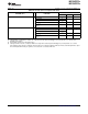
Port P2, P2.5 to P2.6, Input/Output With Schmitt Trigger
Table 47. Port P2 (P2.5 to P2.6) Pin Functions
CONTROL BITS/SIGNALS
PIN NAME (P2.x) x FUNCTION
P2DIR.x P2SEL1.x P2SEL0.x
P2.5/TB0.0/UCA1TXD/UCA1SIMO 5 P2.5(I/O)
(1)
I: 0; O: 1 0 0
TB0.CCI0B
(1)
0
0 1
TB0.0
(1)
1
UCA1TXD/UCA1SIMO
(1)
X
(2)
1 0
P2.6/TB1.0/UCA1RXD/UCA1SOMI 6 P2.6(I/O)
(1)
I: 0; O: 1 0 0
TB1.CCI0B
(1)
0
0 1
TB1.0
(1)
1
UCA1RXD/UCA1SOMI
(1)
X
(2)
1 0
(1) Not available on all devices and package types.
(2) Direction controlled by eUSCI_A1 module.
78 Submit Documentation Feedback Copyright © 2011–2013, Texas Instruments Incorporated